R8C/20 Group, R8C/21 Group 14. Timers
Rev.2.00 Aug 27, 2008 Page 229 of 458
REJ09B0250-0200
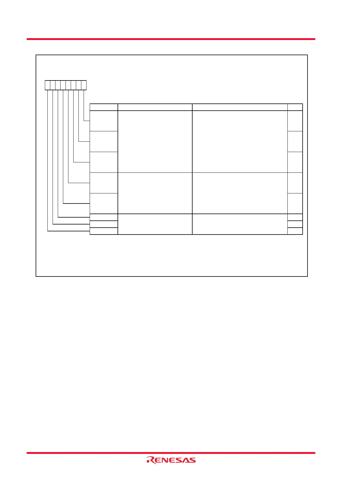
Figure 14.91 Registers TRDCR0 to TRDCR1 in Complementary PWM Mode
Timer RD Control Register i (i = 0 or 1)
Symbol Address After Reset
TRDCR0
TRDCR1
0140h
0150h
00h
00h
Bit Symbol Bit Name Function RW
NOTES:
1.
2.
3.
RW
TCK1 RW
TCK0
RW
RW
RW
CCLR2
CCLR1 RW
Count source selection bit
(2)
b2 b1 b0
0 0 0 : f1
0 0 1 : f2
0 1 0 : f4
0 1 1 : f8
1 0 0 : f32
1 0 1 : TRDCLK input
(1)
1 1 0 : fOCO40M
1 1 1 : Do not set
External clock edge selection bit
(2,3)
b4 b3
0 0 : Count at the rising edge
0 1 : Count at the falling edge
1 0 : Count at both edges
1 1 : Do not set
b7 b6 b5 b4
000
b3 b2
CKEG0
b1 b0
TCK2
This bit is enabled w hen the TCK2 to TCK0 bits are set to 101b (TRDCLK input) and the STCLK bit in the TRDFCR
register is set to 1 (external clock input enabled).
RW
CKEG1
CCLR0 RWSet to 000b (disable clear (free-running
operation)) in complementary PWM mode.
TRDi counter clear selection bit
This bit is enabled w hen the STCLK bit in the TRDFCR register is set to 1 (external clock input enabled).
Set the TCK2 to TCK0 bits and CKEG1 to CKEG0 bits in the TRDCR0 and TRDCR1 registers to the same values.
 Loading...