R8C/20 Group, R8C/21 Group 15. Serial Interface
Rev.2.00 Aug 27, 2008 Page 268 of 458
REJ09B0250-0200
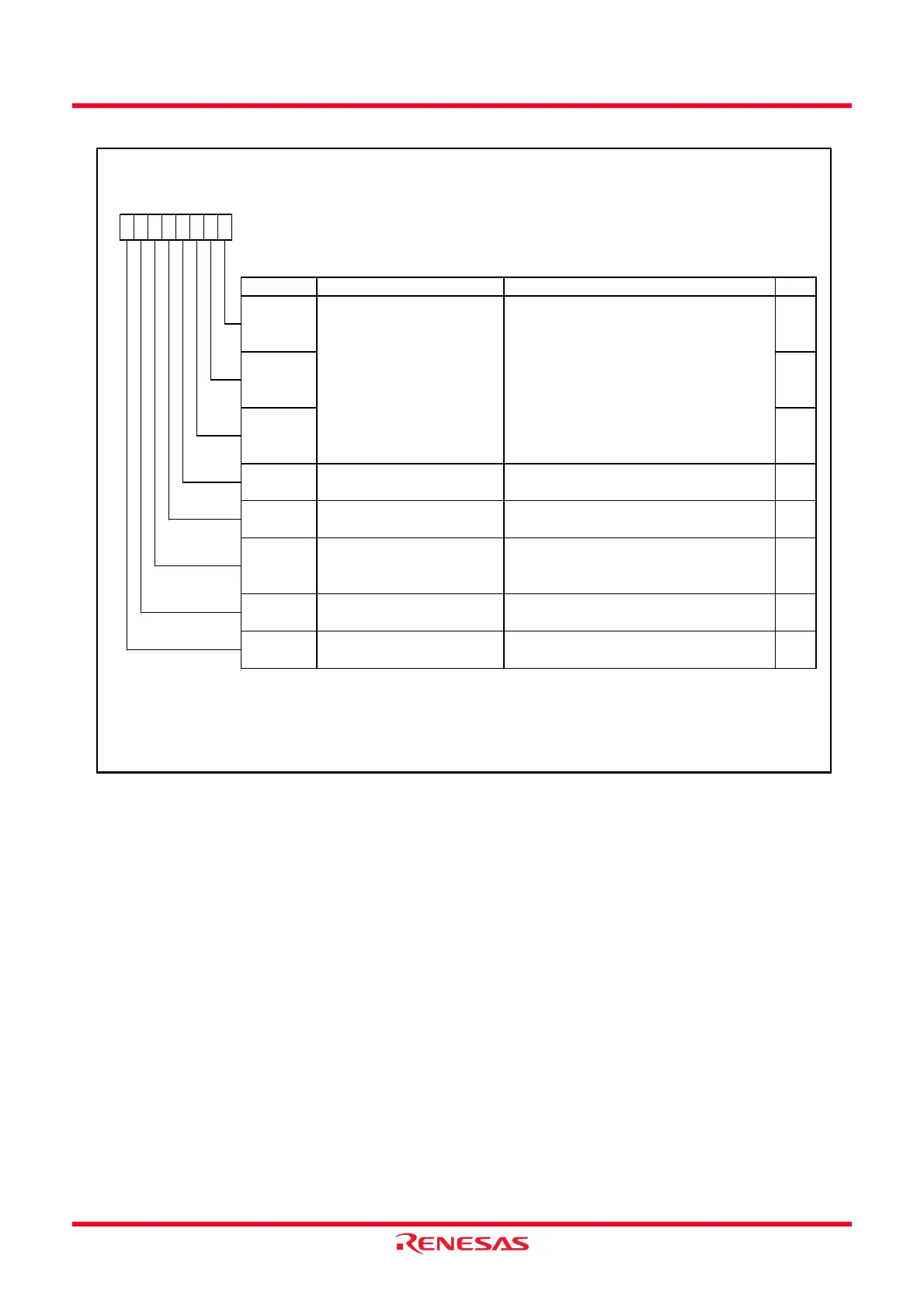
Figure 15.4 UiMR Register (i = 0 or 1)
UARTi Transmit/Receive Mode Register (i = 0 or 1)
Symbol Address After Reset
U0MR 00A0h 00h
U1MR 00A8h 00h
Bit Symbol Bit Name Function RW
NOTES:
1.
2.
3.
4.
Do not set bits SMD2 to SMD0 in the U1MR register to any values other than 000b, 100b, 101b and 110b.
Set the CKDIR bit to 0 (internal clock) in UART1.
The SMD2 to SMD1 bits can not select clock synchronous serial I/O mode in UART1.
Internal/external clock select
bit
(3)
0 : Internal clock
1 : External clock
(1)
Stop bit length select bit
—
(b7)
Reserved bit
RW
Odd/even parity select bit
PRY E
Parity enable bit 0 : Parity disabled
1 : Parity enabled
PRY
RW
Set to 0
Set the PD1_6 bit in the PD1 register to 0 (input).
SMD2 RW
RW
STPS RW
0 : 1 stop bit
1 : 2 stop bits
CKDIR
RW
RW
Serial I/O mode select bit
(2,4)
b2 b1 b0
0 0 0 : Serial interface disabled
0 0 1 : Clock synchronous serial I/O mode
1 0 0 : UART mode transfer data 7 bits long
1 0 1 : UART mode transfer data 8 bits long
1 1 0 : UART mode transfer data 9 bits long
Other than above : Do not set
SMD1
Enables w hen PRYE = 1
0 : Odd parity
1 : Even parity
b7 b6 b5 b4
0
b3 b2 b1 b0
SMD0 RW
 Loading...