R8C/20 Group, R8C/21 Group 20. Electrical Characteristics
Rev.2.00 Aug 27, 2008 Page 426 of 458
REJ09B0250-0200
Timing Requirements (Unless Otherwise Specified: VCC = 3 V, VSS = 0V at Topr = 25°C) [VCC = 3 V]
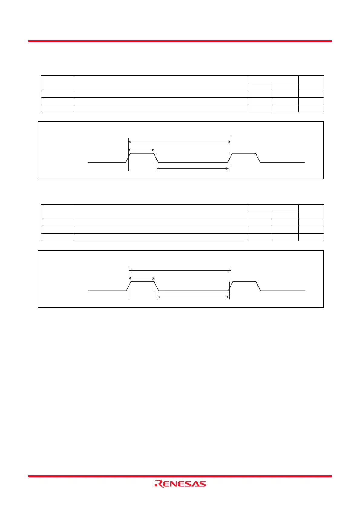
Figure 20.12 XIN Input Timing Diagram when V
CC = 3 V
Figure 20.13 TRAIO Input Timing Diagram when V
CC = 3 V
Table 20.22 XIN
Input
Symbol Parameter
Standard
Unit
Min. Max.
t
c(XIN) XIN input cycle time 100 − ns
t
WH(XIN) XIN input “H” width 40 − ns
t
WL(XIN) XIN input “L” width 40 − ns
Table 20.23 TRAIO Input
Symbol Parameter
Standard
Unit
Min. Max.
t
c(TRAIO) TRAIO input Cycle time 300 − ns
t
WH(TRAIO) TRAIO input “H” width 120 − ns
t
WL(TRAIO) TRAIO input “L” width 120 − ns
Vcc = 3V
XIN input
t
WH(XIN)
tc(XIN)
tWL(XIN)
Vcc = 3V
TRAIO input
t
WH(TRAIO)
tc(TRAIO)
tWL(TRAIO)
 Loading...