R8C/20 Group, R8C/21 Group 7. Programmable I/O Ports
Rev.2.00 Aug 27, 2008 Page 44 of 458
REJ09B0250-0200
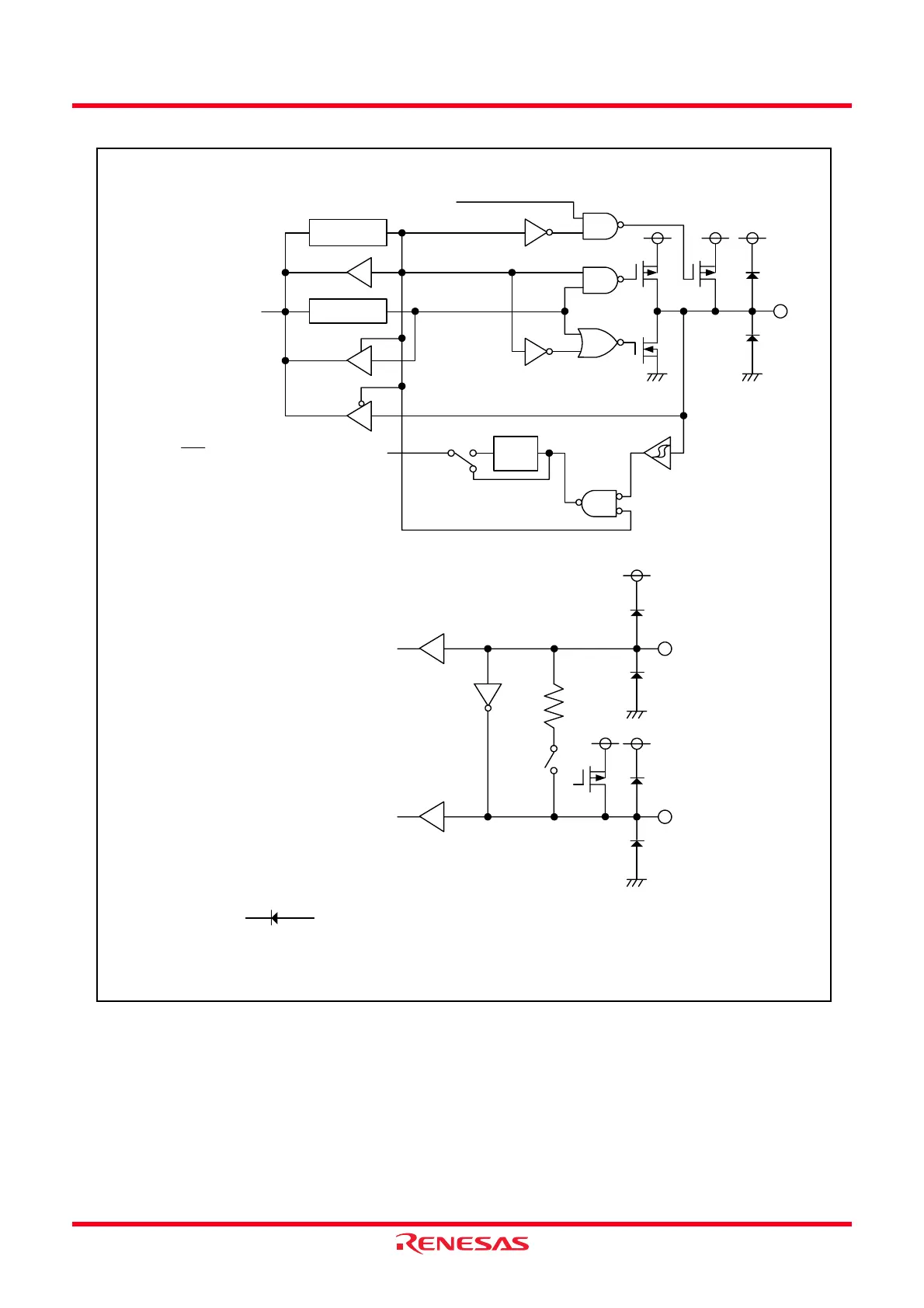
Figure 7.5 Configuration of Programmable I/O Ports (5)
P4_5
INT0 and input to each peripheral function
Port latchData bus
Pull-up selection
Digital
filter
P4_6/XIN
Data bus
Clocked inverter
(2)
P4_7/XOUT
Data bus
(3)
NOTES:
1. symbolizes a parasitic diode.
Ensure the input voltage on each port will not exceed VCC.
2. When CM05 = 1, CM10 = 1, or CM13 = 0, the clocked inverter is cutoff.
3. When CM10 = 1 or CM13 = 0, the feedback resistor is unconnected.
4. When CM05 = CM13 = 1 or CM10 = CM13 = 1, this pin is pulled up.
(4)
Direction
register
(1)
(1)
(1)
(1)
(1)
(1)
 Loading...