R8C/20 Group, R8C/21 Group 10. Clock Generation Circuit
Rev.2.00 Aug 27, 2008 Page 80 of 458
REJ09B0250-0200
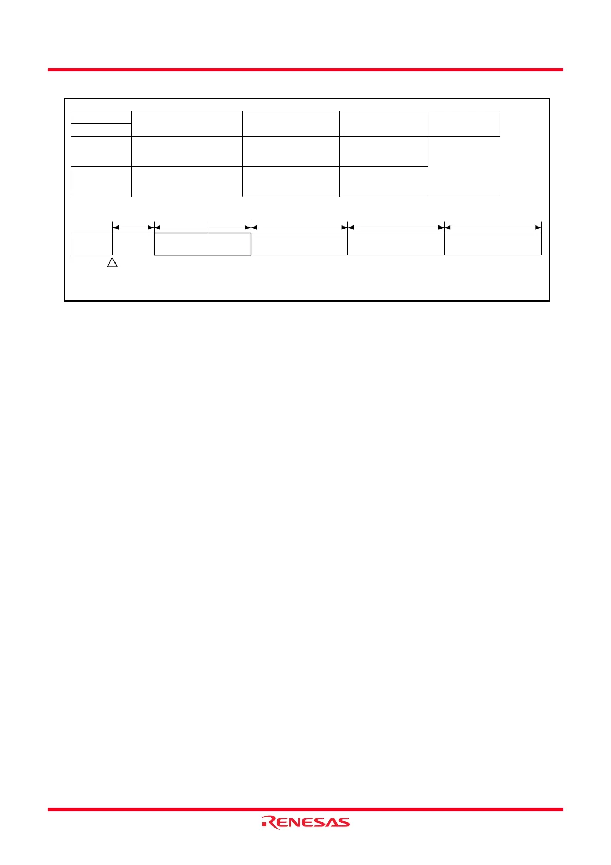
Figure 10.11 Time from Stop Mode to Interrupt Routine Execution
Time until Flash Memory is
Activated (T2)
Time until CPU Clock is
Supplied (T3)
Time for Interrupt
Sequence (T4)
Remarks
0
(flash memory
operates)
Period of system clock
× 12 cycles + 30 µs (max.)
Period of CPU clock
× 6 cycles
Period of CPU clock
× 20 cycles
Following total
time of T0 to T4 is
the time from wait
mode until an
interrupt routine is
executed.
1
(flash memory
stops)
Period of system clock
× 12 cycles
Same as above Same as above
Stop
mode
Flash memory activation
sequence
CPU clock restart
sequence
Interrupt sequence
T2 T3 T4
Interrupt
request
generated
Oscillation period of the CPU
clock source used immediately
before stop mode
T1
Internal
power
stability time
150 µs
(max.)
T0
FMR0 Register
FMSTP Bit
 Loading...