R8C/1A Group, R8C/1B Group 16. Clock Synchronous Serial Interface
Rev.1.30 Dec 08, 2006 Page 172 of 315
REJ09B0252-0130
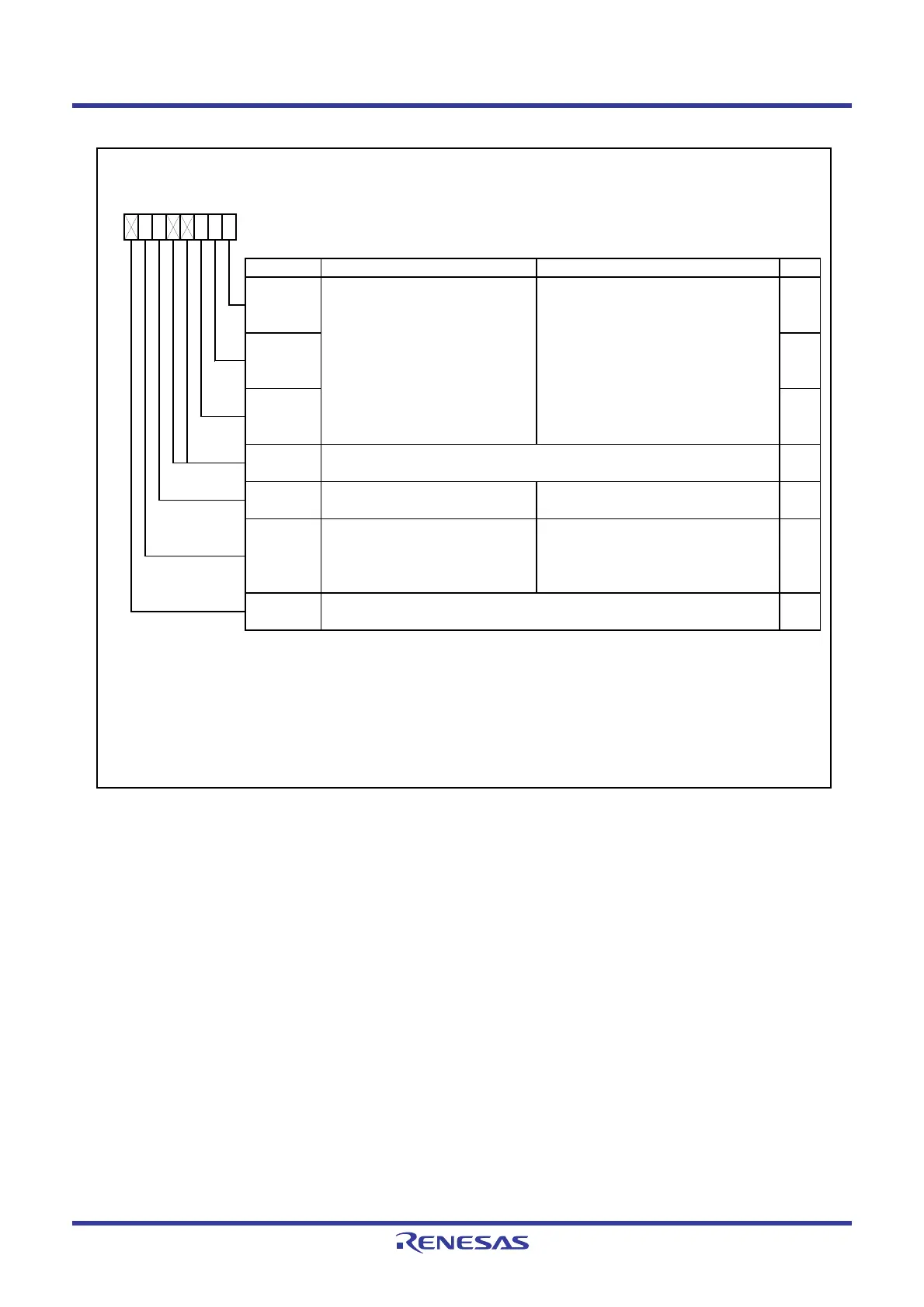
Figure 16.2 SSCRH Register
SS Control Register H
(4)
Symbol Address After Reset
SSCRH
00B8h 00h
Bit Symbol Bit Name Function RW
NOTES :
1.
2.
3.
4. Refer to
16.2.8.1 Accessing Registers Associated with Clock Synchronous Serial I/O with Chip Select
for
more information.
The RSSTP bit is disabled w hen the MSS bit is set to 0 (operates as slave device).
b7 b6 b5 b4 b3 b2 b1 b0
RW
RW
RW
—
(b4-b3)
—
Nothing is assigned. If necessary, set to 0.
When read, the content is 0.
CKS1
CKS2
Transfer clock rate select bits
(1)
b2 b1 b0
0 0 0 : f1/256
0 0 1 : f1/128
0 1 0 : f1/64
0 1 1 : f1/32
1 0 0 : f1/16
1 0 1 : f1/8
1 1 0 : f1/4
1 1 1 : Do not set.
CKS0
Master/slave device select bit
(2)
0 : Operates as slave device.
1 : Operates as master device.
RWMSS
The SSCK pin functions as the transfer clock output pin w hen the MSS bit is set to 1 (operates as master device).
The MSS bit is set to 0 (operates as slave device) w hen the CE bit in the SSSR register is set to 1 (conflict error
occurs).
RSSTP
Receive single stop bit
(3)
0 : Maintains receive operation after
receiving 1 byte of data.
1 : Completes receive operation after
receiving 1 byte of data.
RW
—
(b7)
Nothing is assigned. If necessary, set to 0.
When read, the content is 0.
The set clock is used w hen the internal clock is selected.
—
 Loading...


