R8C/1A Group, R8C/1B Group 16. Clock Synchronous Serial Interface
Rev.1.30 Dec 08, 2006 Page 174 of 315
REJ09B0252-0130
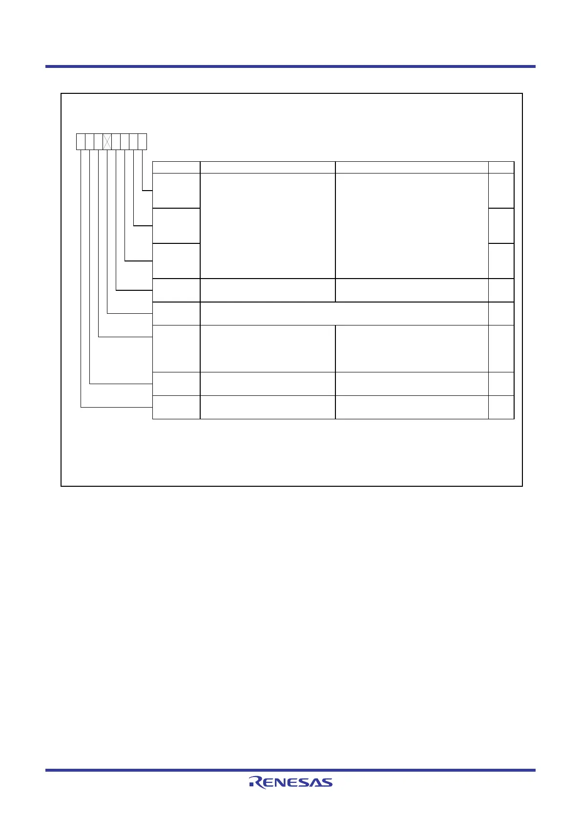
Figure 16.4 SSMR Register
SS Mode Register
(2)
Symbol Address After Reset
SSMR
00BAh 00011000b
Bit Symbol Bit Name Function RW
Reserved bit
NOTES :
1.
2. Refer to
16.2.8.1 Accessing Registers Associated with Clock Synchronous Serial I/O with Chip Select
for
more information.
0 : “H” w hen clock stops.
1 : “L” w hen clock stops.
Set to 1.
When read, the content is 1.
RW
RW
RW
—
RW
0 : Transfers data MSB first.
1 : Transfers data LSB first.
Ref er to
16.2.1.1 Association between Transfer Clock Polarity, Phase and Data
for the settings of bits CPHS
and CPOS.
R
BC1
BC2
Bit counter 2 to 0
b2 b1 b0
0 0 0 : 8 bits left
0 0 1 : 1 bit left
0 1 0 : 2 bits left
0 1 1 : 3 bits left
1 0 0 : 4 bits left
1 0 1 : 5 bits left
1 1 0 : 6 bits left
1 1 1 : 7 bits left
BC0
R
R
SSCK clock phase select bit
(1)
0 : Change data at odd edge
(Dow nload data at even edge).
1 : Change data at even edge
(Dow nload data at odd edge).
CPOS
SSCK clock polarity select bit
(1)
b7 b6 b5 b4 b3 b2 b1 b0
1
MSB first/LSB first select bit
MLS
Nothing is assigned. If necessary, set to 0.
When read, the content is 1.
—
(b3)
—
(b4)
CPHS
 Loading...


