R8C/1A Group, R8C/1B Group 19. Electrical Characteristics
Rev.1.30 Dec 08, 2006 Page 281 of 315
REJ09B0252-0130
NOTES:
1. This condition is not applicable when using with Vcc
≥ 1.0 V.
2. When turning power on after the time to hold the external power below effective voltage (V
por1) exceeds10 s, refer to Table
19.9 Reset Circuit Electrical Characteristics (When Not Using Voltage Monitor 1 Reset)
.
3. t
w(por2) is the time to hold the external power below effective voltage (Vpor2).
NOTES:
1. When not using voltage monitor 1, use with Vcc
≥ 2.7 V.
2. t
w(por1) is the time to hold the external power below effective voltage (Vpor1).
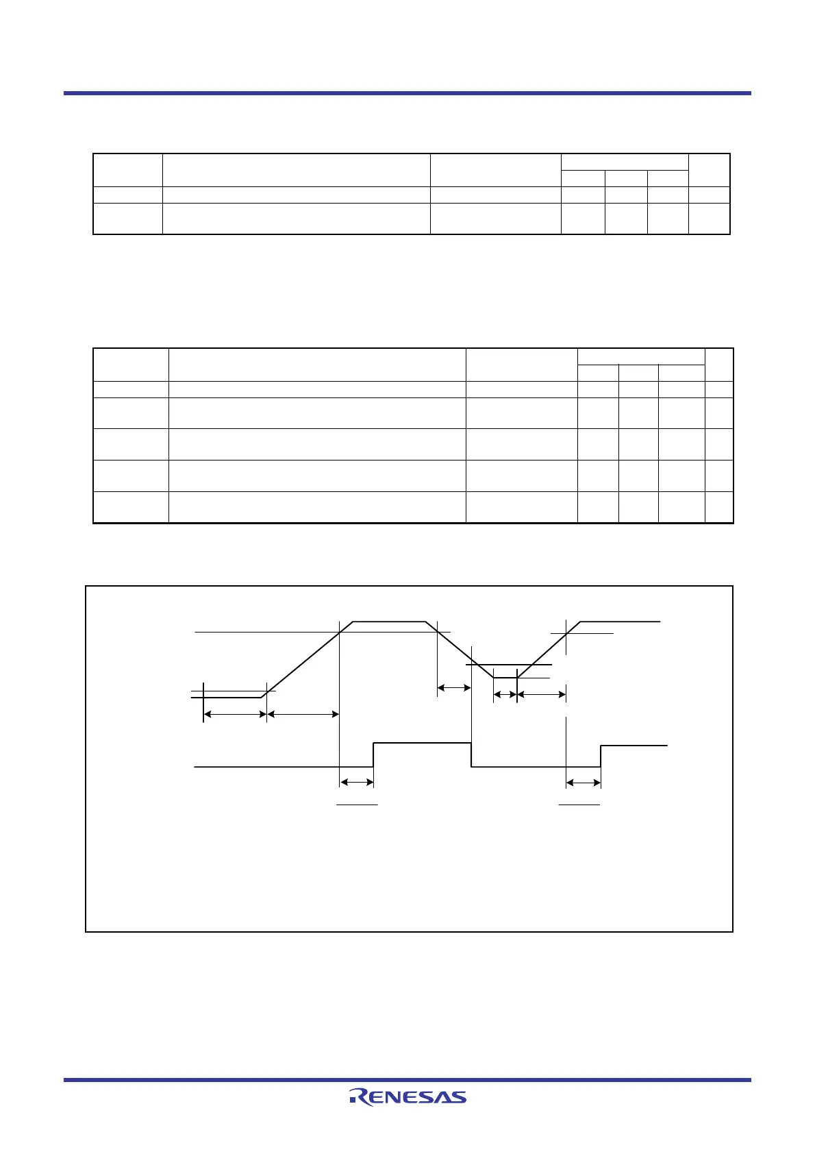
Figure 19.3 Reset Circuit Electrical Characteristics
Table 19.8 Reset Circuit Electrical Characteristics (When Using Voltage Monitor 1 Reset)
Symbol Parameter Condition Standard Unit
Min. Typ. Max.
V
por2 Power-on reset valid voltage -20°C ≤ Topr ≤ 85°C −−Vdet1 V
t
w(Vpor2-Vdet1) Supply voltage rising time when power-on reset is
deasserted
(1)
-20°C ≤ Topr ≤ 85°C,
t
w(por2) ≥ 0s
(3)
−−100 ms
Table 19.9 Reset Circuit Electrical Characteristics (When Not Using Voltage Monitor 1 Reset)
Symbol Parameter Condition Standard Unit
Min. Typ. Max.
V
por1 Power-on reset valid voltage -20°C ≤ Topr ≤ 85°C −−0.1 V
t
w(Vpor1-Vdet1) Supply voltage rising time when power-on reset is
deasserted
0°C ≤ Topr ≤ 85°C,
t
w(por1) ≥ 10 s
(2)
−−100 ms
t
w(Vpor1-Vdet1) Supply voltage rising time when power-on reset is
deasserted
-20°C ≤ Topr < 0°C,
t
w(por1) ≥ 30 s
(2)
−−100 ms
t
w(Vpor1-Vdet1) Supply voltage rising time when power-on reset is
deasserted
-20°C ≤ Topr < 0°C,
t
w(por1) ≥ 10 s
(2)
−− 1ms
t
w(Vpor1-Vdet1) Supply voltage rising time when power-on reset is
deasserted
0°C ≤ Topr ≤ 85°C,
t
w(por1) ≥ 1 s
(2)
−−0.5 ms
NOTES:
1. Hold the voltage inside the MCU operation voltage range (Vccmin or above) within the sampling time.
2. The sampling clock can be selected. Refer to 7. Voltage Detection Circuit for details.
3. V
det1 indicates the voltage detection level of the voltage detection 1 circuit. Refer to 7. Voltage Detection Circuit for details.
V
det1
(3)
Vpor1
Internal reset signal
(“L” valid)
t
w(por1)
tw(Vpor1–Vdet1)
Sampling time
(1, 2)
Vdet1
(3)
1
f
RING-S
× 32
1
f
RING-S
× 32
Vpor2
Vccmin
tw(por2) tw(Vpor2–Vdet1)
 Loading...


