RH850/F1K Series Hardware Design Guide
R01AN2911EJ0100 Rev. 1.00 Page 10 of 46
Aug 04, 2016
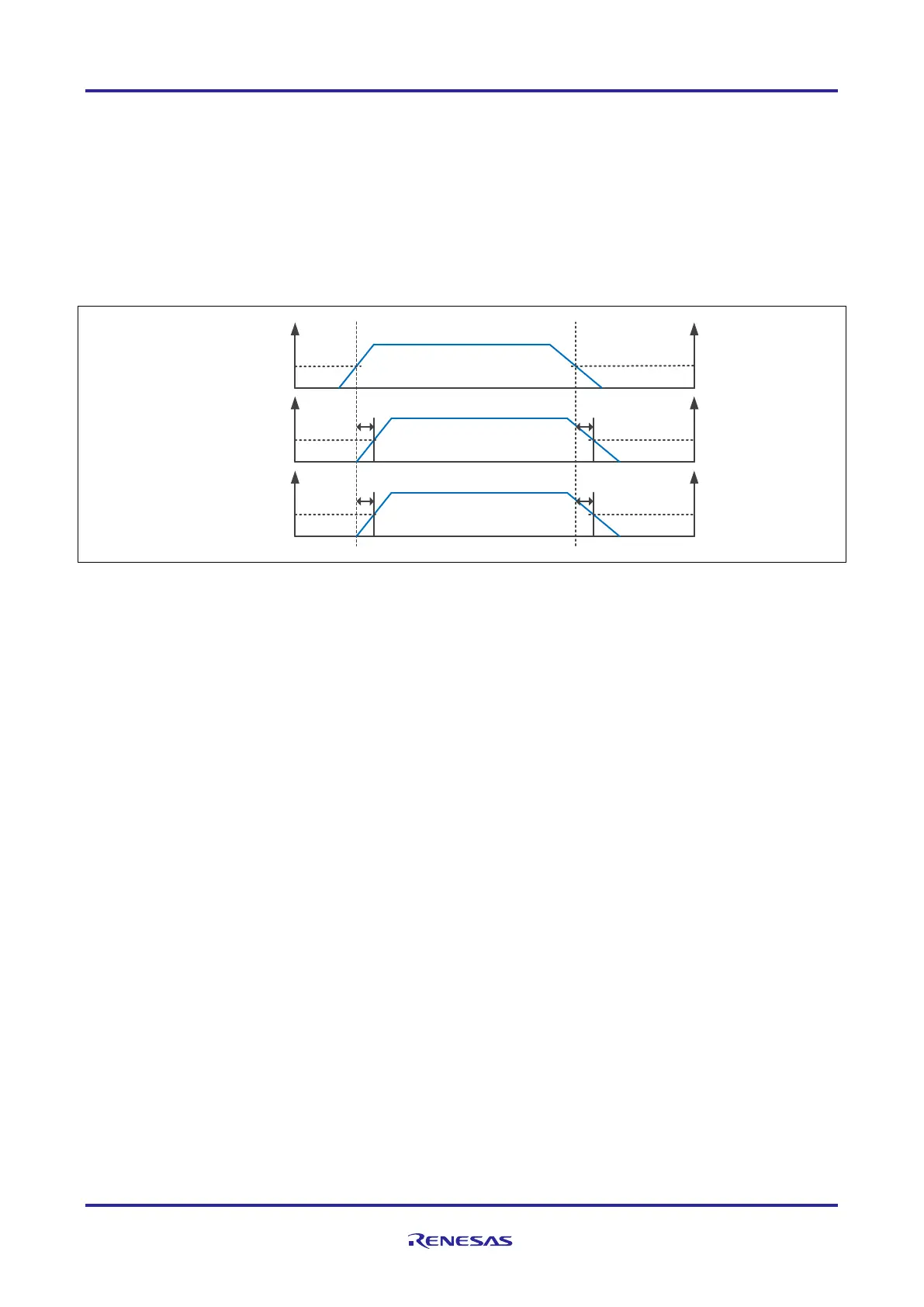
1.1.4 Power Supply Timing of RH850/F1K Group
The RH850/F1K group has a recommended power supply timing.
The voltage slope of the different power supply pins is defined with min. 0.02V/ms and max. 500V/ms.
For details on the electrical characteristics, please refer to the corresponding device RH850/F1K hardware user’s
manual.
Figure 2 RH850/F1K Power up/down timing
Note: tVS is the timing of the voltage slope
REGVCC/EVCC
2.7V
2.7V
A0VREF
A1VREF
3.0V
3.0V 3.0V
3.0V
0V
0V
0V
0V
0V
0V
tr3 = min. 0µs, max. 60µs
tr4 = min. 0µs, max. 60µs
tf3 = max. 0.5/tVS
tf4 = max. 0.5/tVS
 Loading...