RH850/F1K Series Hardware Design Guide
R01AN2911EJ0100 Rev. 1.00 Page 16 of 46
Aug 04, 2016
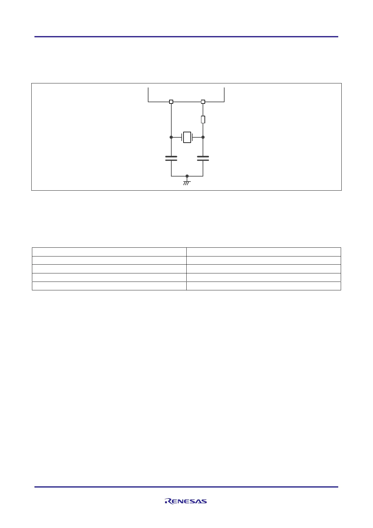
3.1.2 Sub Oscillator
A crystal resonator can be connected to the sub clock input pins as shown below.
Figure 6 Recommended sub oscillator circuit
General guidance values of the sub oscillator circuit:
Table 10 Guidance values of the sub oscillator circuit
Caution
Values of C1S, C2S and RdS depend on the crystal resonator used and must be specified in cooperation with a
crystal resonator manufacturer.
3.2 Recommended Oscillator Layout
General guidance for PCB layout:
• Keep the wiring length as short as possible
• Do not cross the wiring with other signal lines
• Do not route this circuit close to a signal line with high fluctuating current flow
• Always make the ground point of the oscillator capacitor the same potential as AWOVSS
• Do not ground the capacitor to a ground pattern with high current flow
• Do not tap signals from the oscillator
For further layout, related recommendations please refer to the application note “PCB-Design for Improved EMC”
(R01AN0733EDxxxx).
RdS
XT1 IP0_0
SOSC
C2SC1S
internal
external
 Loading...