RH850/F1K Series Hardware Design Guide
R01AN2911EJ0100 Rev. 1.00 Page 32 of 46
Aug 04, 2016
6.1 Development Tool Interface of RH850/F1K Group
The description of the development tool interface in this chapter assumes that the normal operating mode of the MCU is
used. When the user boot mode shall be used the configuration of the pins FLMD0, P10_8/FLMD1, P10_1/MODE0,
P10_2/MODE1 and P10_6/MODE2 has to be set accordingly.
6.1.1 Debug Interface Connection of RH850/F1K Group
For the debugging environment, the following interface connections are supported:
1pin Low-pin debug interface (1pin LPD)
4pin Low-pin debug interface (4pin LPD)
Nexus interface
o The Nexus interface is only supported by 3rd party development tools.
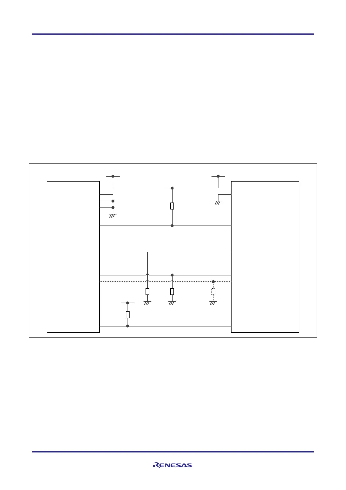
Figure 15 RH850/F1K 1pin Low-pin debug interface connection
Note: The maximum sink current of the RESET terminal of the E1 emulator is 2mA. The external pull-up circuit of
the RESET pin has to be considered based on the applications requirement. When an external RESET
component is used, the pull-up resistor value has to be selected appropriately.
When the 1pin debug mode is used on the RH850/F1K group, the port of the JP0 port group is automatically switched
to the debug interface mode. The remaining pins of JP0 can be used as general-purpose I/O pin including its alternate
function.
JP0_0: LPDIO input/output
JP0_1: General-purpose I/O
JP0_2: General-purpose I/O
JP0_3: General-purpose I/O
TVDD
GND
GND
GND
VDDVDD
EVCC
EVSS
TDI/LPDIO
FPMD0
FPMD1
RESET RESET
P10_8 (FLMD1)
FLMD0
JP0_0 (DCUTDI/LPDIO, LPDI)
VDD
1k to 4.7kΩ
RH850/F1K Group
E1 Emulator
(14pin Connector)
100kΩ
1k to 10kΩ
10k to 100kΩ
JP0_4 (DCUTRST)
VDD
min. 4.7kΩ
Note
 Loading...