RH850/F1K Series Hardware Design Guide
R01AN2911EJ0100 Rev. 1.00 Page 34 of 46
Aug 04, 2016
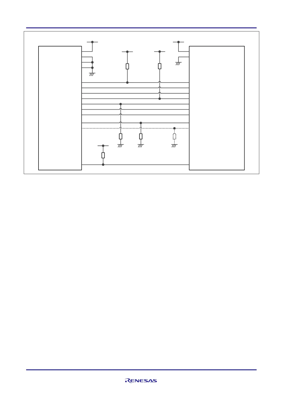
Figure 17 RH850/F1K Nexus, 4pin LPD and 1pin LPD debug interface connection
The use of an external resistor is only required when the Nexus IF mode is used for debugging
and depends on the hardware specification and implementation of the 3
rd
party development tool.
When the Nexus interface is used for debugging the value of the resistor depends on the 3
rd
party
development tool specification.
The resistor is optional when the 4pin low-pin debug mode is used
The maximum sink current of the RESET terminal of the E1 emulator is 2mA. The external pull-
up circuit of the RESET pin has to be considered based on the applications requirement. When an
external RESET component is used, the pull-up resistor value has to be selected appropriately.
When the Nexus debug mode is used on the RH850/F1K group, the ports of the JP0 port group are automatically
switched to the debug interface mode.
JP0_0: DCUTDI input
JP0_1: DCUTDO output
JP0_2: DCUTCK input
JP0_3: DCUTMS input
JP0_4: DCUTRST input
JP0_5: DCUTRDY output
JP0_6: EVTO
TVDD
GND
GND
GND
VDD
VDD
EVCC
EVSS
TDI/LPDIO
TDO/LPDO
TCK/LPDCLK
TMS
TRST
RDY/LPDCLKOUT
FPMD0
FPMD1
RESET RESET
P10_8 (FLMD1)
FLMD0
JP0_0 (DCUTDI/LPDIO, LPDI)
JP0_1 (DCUTDO/LPDO)
JP0_2 (DCUTCK/LPDCLK)
JP0_3 (DCUTMS)
JP0_4 (DCUTRST)
JP0_5 (DCURDY/LPDCLKOUT)
VDD
1k to 4.7kΩ
Note 3
RH850/F1K Group
E1 Emulator
(14pin Connector)
100kΩ
1k to 10kΩ
EVTO JP0_6 (EVTO)
VDD
Note 1
10k to 100kΩ
Note 2
VDD
min. 4.7kΩ
Note 4
 Loading...