RH850/F1K Series Hardware Design Guide
R01AN2911EJ0100 Rev. 1.00 Page 29 of 46
Aug 04, 2016
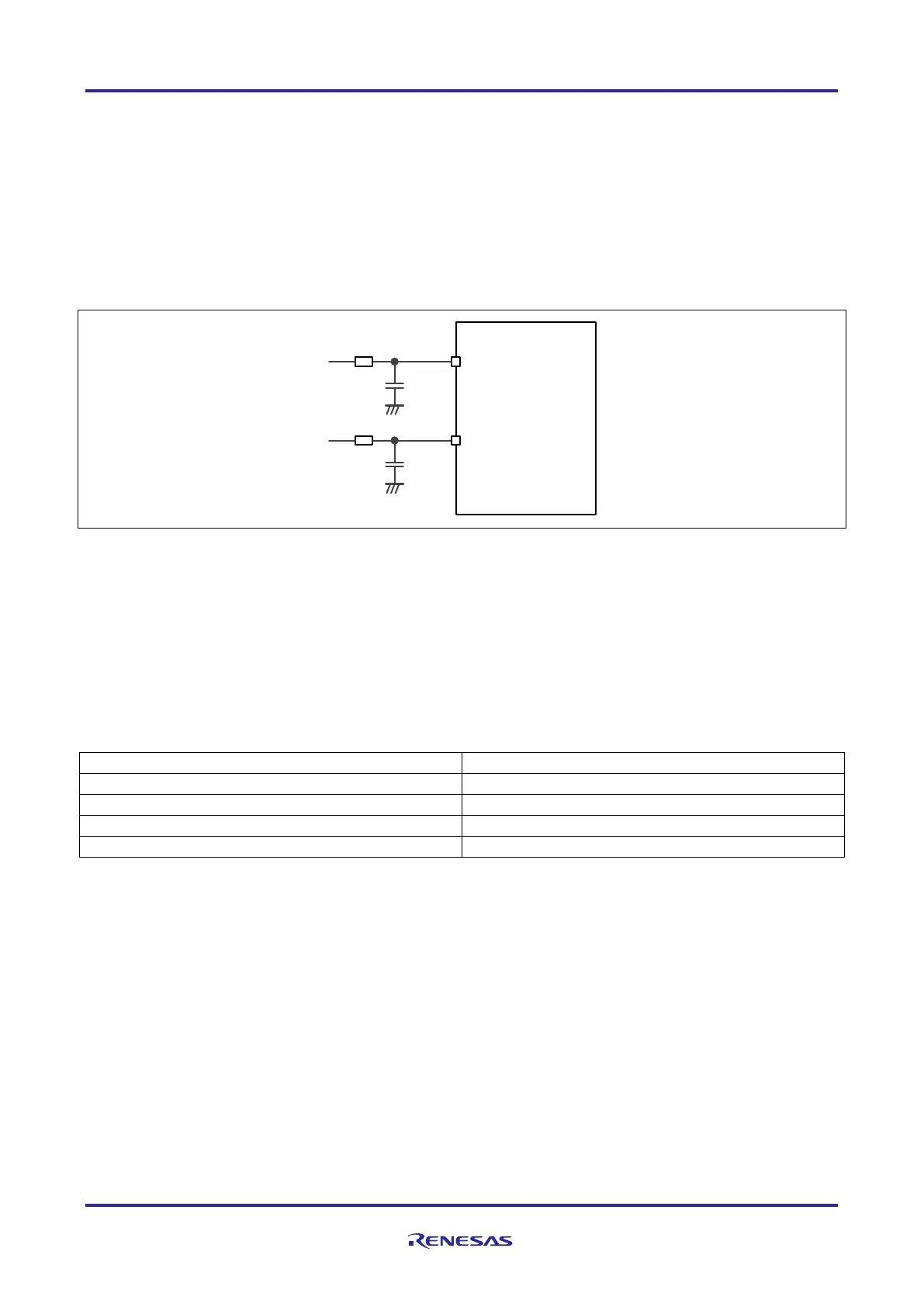
5.4 External Circuit on ADC Input
To preserve the accuracy of the A/D-converter, it is recommended that analog input pins have a low impedance.
Therefore placing a capacitor at the analog input pin can provide an effective result. This capacitor contributes to noise
filtering on the analog input pin. A basic filter can be realized by using a series resistor with a capacitor on the input pin
(RC-filter).
The filter at the input pins should be designed taking into account the dynamic characteristics of the input signal, the
equivalent input impedance of the ADC itself and the injected current specification of the analog input pins.
Figure 14 ADC external circuit on analog input
RH850/F1K Group (max. device configuration)
n = 0, m = 0 to 15, 0S to 19S
n = 1, m = 0 to 15, 0S to 7S
General guidance values of the basic external ADC input circuit:
Table 18 Basic external ADC input circuit
The values of the resistor and capacitor depend on the application requirements.
In order to improve the electromagnetic susceptibility it should be considered to add a series resistor (R1) to the supply
line of AnVREF. The combination of series resistor and capacitor (C1) placed close to the supply pin AnVREF helps to
improve the resistance against electromagnetic disturbance.
The resistor value influences the conversion accuracy and depends on the application requirements.
In order to improve the accuracy of the ADC it is recommended to add a capacitor of minimum 2µF (typical 4.7µF) in
parallel to the capacitor C1 at AnVREF. The value and PCB placement of the parallel capacitor depends on the
application requirements.
ADCAnIm, ADCAnImS
RH850/F1K
R2
C2
AnVREF
C1
R1
 Loading...