EasyManuals Logo

Renesas RH850/F1K Series User Manual

Renesas RH850/F1K Series
49 pages
To Next Page IconTo Next Page
To Previous Page IconTo Previous Page
Page #28 background imageLoading...
Page #28 background image
RH850/F1K Series Hardware Design Guide
R01AN2911EJ0100 Rev. 1.00 Page 28 of 46
Aug 04, 2016
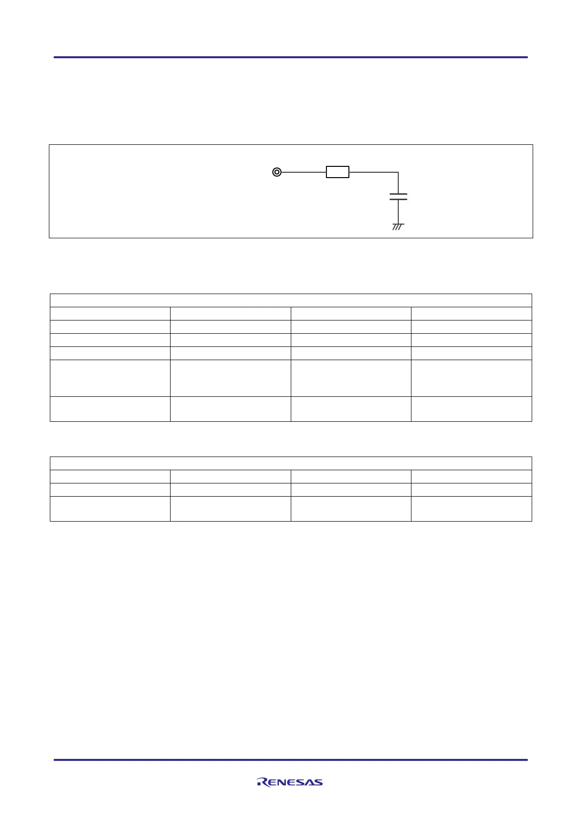
5.3 Equivalent Input Circuit
The A/D-converters have different options for the input with track & hold path or direct path only. Please refer to the
user’s manual, which A/D-converter is supported by the chosen device.
Figure 13 ADC equivalent input circuit
Table 16 Equivalent input circuit of ADCA0
ADCA0
Terminals
Condition
RIN [kΩ]
CIN [pF]
ADCA0I0 to ADCA0I5
Channel T&H is not used
3.9
2.1
ADCA0I0 to ADCA0I5
Channel T&H is used
14.0
1.8
ADCA0I6 to ADCA0I15
3.9
2.1
ADCA0I0S to
ADCA0I3S, ADCA0I5S
to ADCA0I16S
5.0
8.6
ADCA0I4S, ADCA0I17S
to ADCA0I19S
5.4
8.6
Table 17 Equivalent input circuit of ADCA1
ADCA1
Terminals
Condition
RIN [kΩ]
CIN [pF]
ADCA1I0 to ADCA1I15
3.6
1.8
ADCA1I0S to
ADCA1I17S
4.7
4.5
Caution
These specifications are not tested during outgoing inspection. Therefore, RIN and CIN are reference values only
and not guaranteed. In addition, these values are specified as maximum values.
ADCAnIm or ADCAnImS
RIN
CIN

Table of Contents

Questions and Answers:

Question and Answer IconNeed help?

Do you have a question about the Renesas RH850/F1K Series and is the answer not in the manual?

Renesas RH850/F1K Series Specifications

General IconGeneral
BrandRenesas
ModelRH850/F1K Series
CategoryPower Supply
LanguageEnglish