RH850/F1K Series Hardware Design Guide
R01AN2911EJ0100 Rev. 1.00 Page 33 of 46
Aug 04, 2016
JP0_4: General-purpose I/O
JP0_5: General-purpose I/O
JP0_6: General-purpose I/O
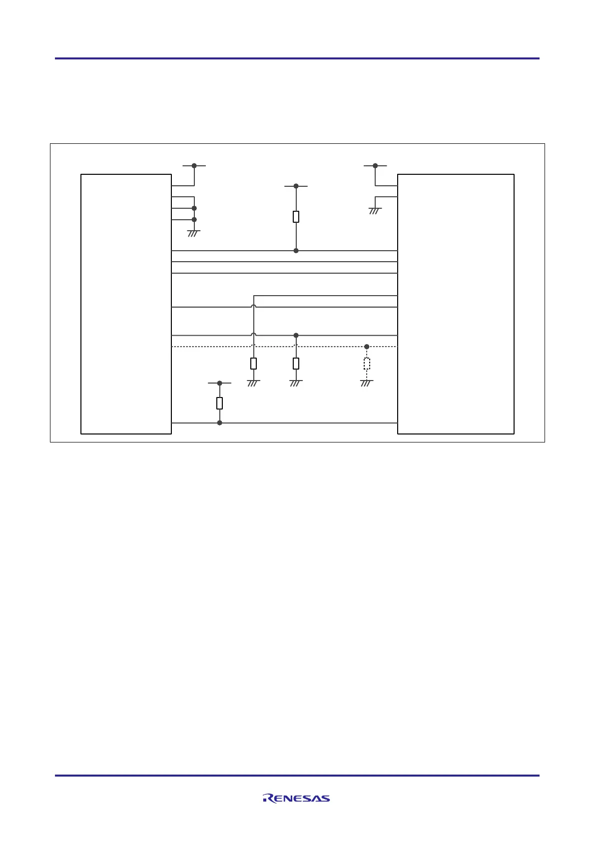
Figure 16 RH850/F1K 4pin Low-pin debug interface connection
The resistor is optional in 4pin low-pin debug mode.
The maximum sink current of the RESET terminal of the E1 emulator is 2mA. The external pull-
up circuit of the RESET pin has to be considered based on the applications requirement. When an
external RESET component is used, the pull-up resistor value has to be selected appropriately.
When the 4pin debug mode is used on the RH850/F1K group, the ports of the JP0 port group are automatically switched
to the debug interface mode. The remaining pins of JP0 can be used as general-purpose I/O pin including its alternate
function.
JP0_0: LPDI input
JP0_1: LPDO output
JP0_2: LPDCLK input
JP0_3: General-purpose I/O
JP0_4: General-purpose I/O
JP0_5: LPDCLKOUT output
JP0_6: General-purpose I/O
TVDD
GND
GND
GND
VDDVDD
EVCC
EVSS
TDI/LPDIO
TDO/LPDO
TCK/LPDCLK
RDY/LPDCLKOUT
FPMD0
FPMD1
RESET RESET
P10_8 (FLMD1)
FLMD0
JP0_0 (DCUTDI/LPDIO, LPDI)
JP0_1 (DCUTDO/LPDO)
JP0_2 (DCUTCK/LPDCLK)
JP0_5 (DCURDY/LPDCLKOUT)
RH850/F1K Group
E1 Emulator
(14pin Connector)
100kΩ
1k to 10kΩ
VDD
1k to 4.7kΩ
Note 1
10k to 100kΩ
JP0_4 (DCUTRST)
VDD
min. 4.7kΩ
Note 2
 Loading...