RH850/F1K Series Hardware Design Guide
R01AN2911EJ0100 Rev. 1.00 Page 40 of 46
Aug 04, 2016
6.1.4 Debug and Flash Programming Interface Connection of RH850/F1K Group when
the internal HSOSC is used as Clock Supply
When the devices of the RH850/F1K group are supply only with the internal high-speed oscillator (HSOSC) the
following functions are supported
4pin Low-pin debug interface (4pin LPD)
Synchronous flash programming interface with PG-FP5
The debugging by 1pin Low pin debug interface (1pin LPD) and the flash programming by UART interface is
not supported when the internal HSOSC is used as clock supply.
The E1 emulator does not support the flash programming through CSI. A programmer that supports the CSI
(e.g. PG-FP5) has to be used for flash programming.
When the debugging is started with a blank device the option byte to select the 4-pin LPD interface has to be set
in advance by using the flash programmer PG-FP5 that supports the flash programming by CSI interface.
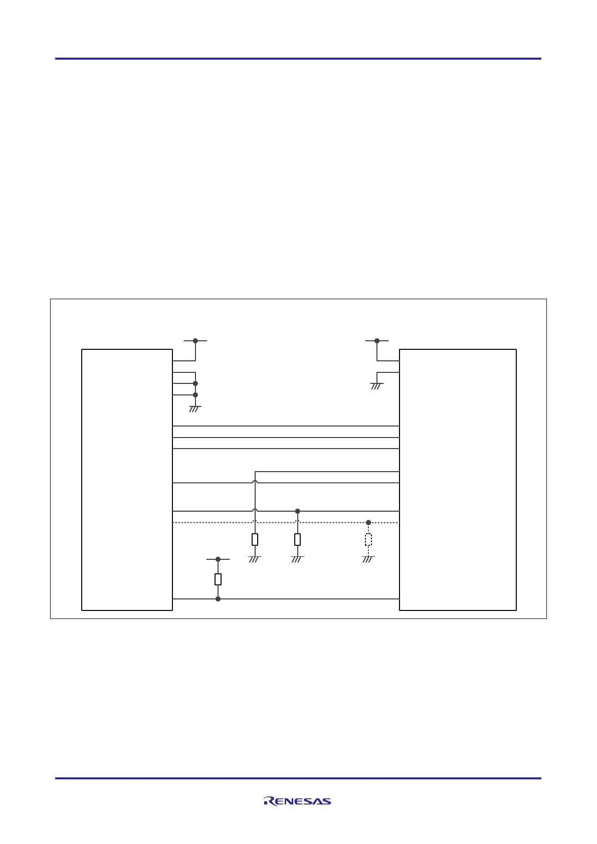
Figure 21 RH850/F1K Debug and flash programming interface connections when the HSOSC is used
as clock supply
The maximum sink current of the RESET terminal of the E1 emulator is 2mA. The external pull-
up circuit of the RESET pin has to be considered based on the applications requirement. When an
external RESET component is used, the pull-up resistor value has to be selected appropriately.
When the 4pin debug mode is used on the RH850/F1K group, the ports of the JP0 port group are automatically switched
to the debug interface mode. The remaining pins of JP0 can be used as general-purpose I/O pin including its alternate
function.
TVDD
GND
GND
GND
VDDVDD
EVCC
EVSS
TDI/LPDIO/TxD/SO
TDO/LPDO/SI
TCK/LPDCLK/SCK
RDY/LPDCLKOUT
FPMD0
FPMD1
RESET RESET
P10_8 (FLMD1)
FLMD0
JP0_0 (TDI/LPDIO, LPDI)
JP0_1 (DCUTDO/LPDO)
JP0_2 (DCUTCK/LPDCLK)
JP0_4 (DCUTRST)
JP0_5 (DCURDY/LPDCLKOUT)
RH850/F1K Group
E1 Emulator
/
PG-FP5 Flash Programmer
(14pin Connector)
100kΩ
1k to 10kΩ
RDY/LPDCLKOUT
10k to 100kΩ
VDD
min. 4.7kΩ
Note 1
 Loading...