RH850/F1K Series Hardware Design Guide
R01AN2911EJ0100 Rev. 1.00 Page 37 of 46
Aug 04, 2016
(a) Flash Programming by PG-FP5
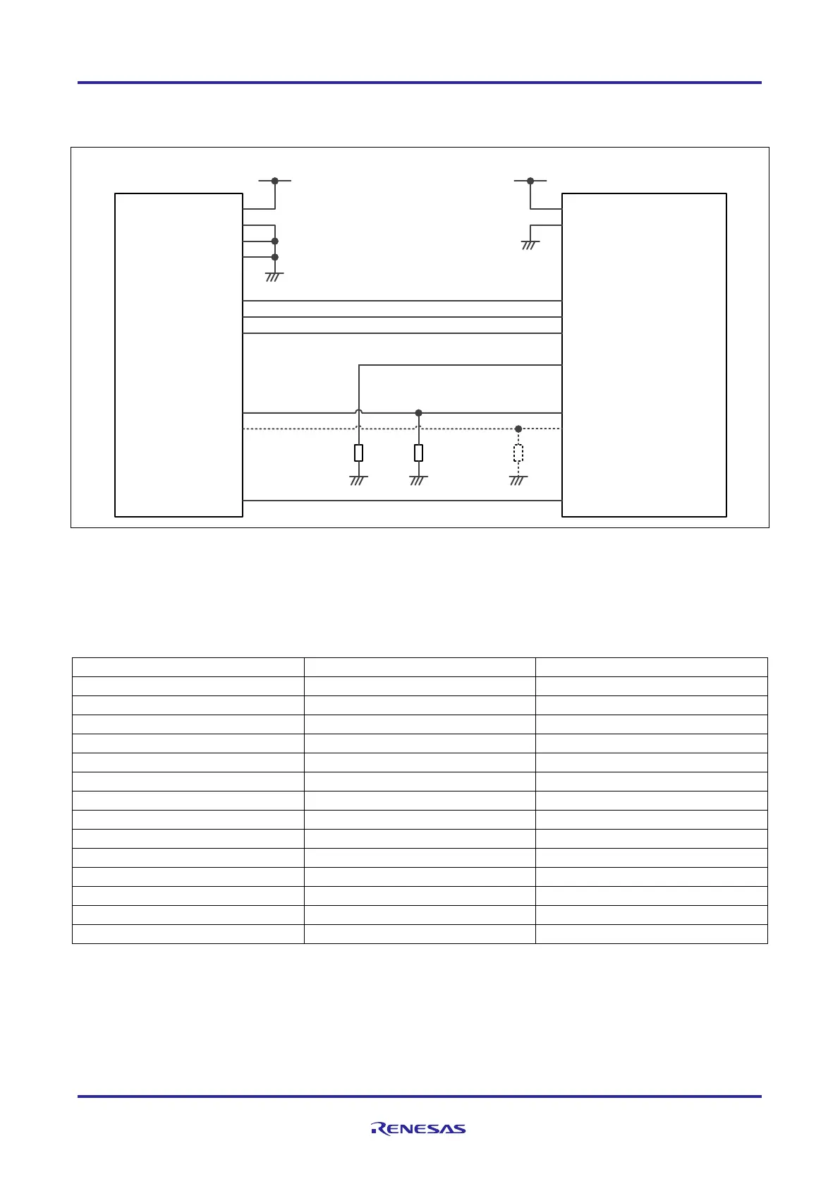
Figure 18 RH850/F1K PG-FP5 flash programming interface connection
The flash programming signal connection of the PG-FP5 interface is given in the table below:
Table 23 PG-FP5 Flash programming signal connection of RH850/F1K
PG-FP5 Interface Connector
Caution:
When alternate port functions of P10_8/FLMD1 are used, please make sure not to drive a high level at reset.
When alternate port functions with pull-up resistor are used, please connect P10_8/FLMD1 to FPMD1 of
emulator. In that case, it is kept at a low level by the emulator when the reset signal is released.
VDD
GND
GND
GND
VDDVDD
EVCC
EVSS
RxD/TxD/SO
RxD/SI
SCK
FPMD0
FPMD1
RESET RESET
P10_8 (FLMD1)
FLMD0
JP0_0 (RxD/TxD/SI)
JP0_1 (TxD/SO)
JP0_2 (SCK)
RH850/F1K Group
PG-FP5 Flash Programmer
(14pin Connector)
100kΩ
1k to 10kΩ
JP0_4
10k to 100kΩ
 Loading...