RH850/F1K Series Hardware Design Guide
R01AN2911EJ0100 Rev. 1.00 Page 13 of 46
Aug 04, 2016
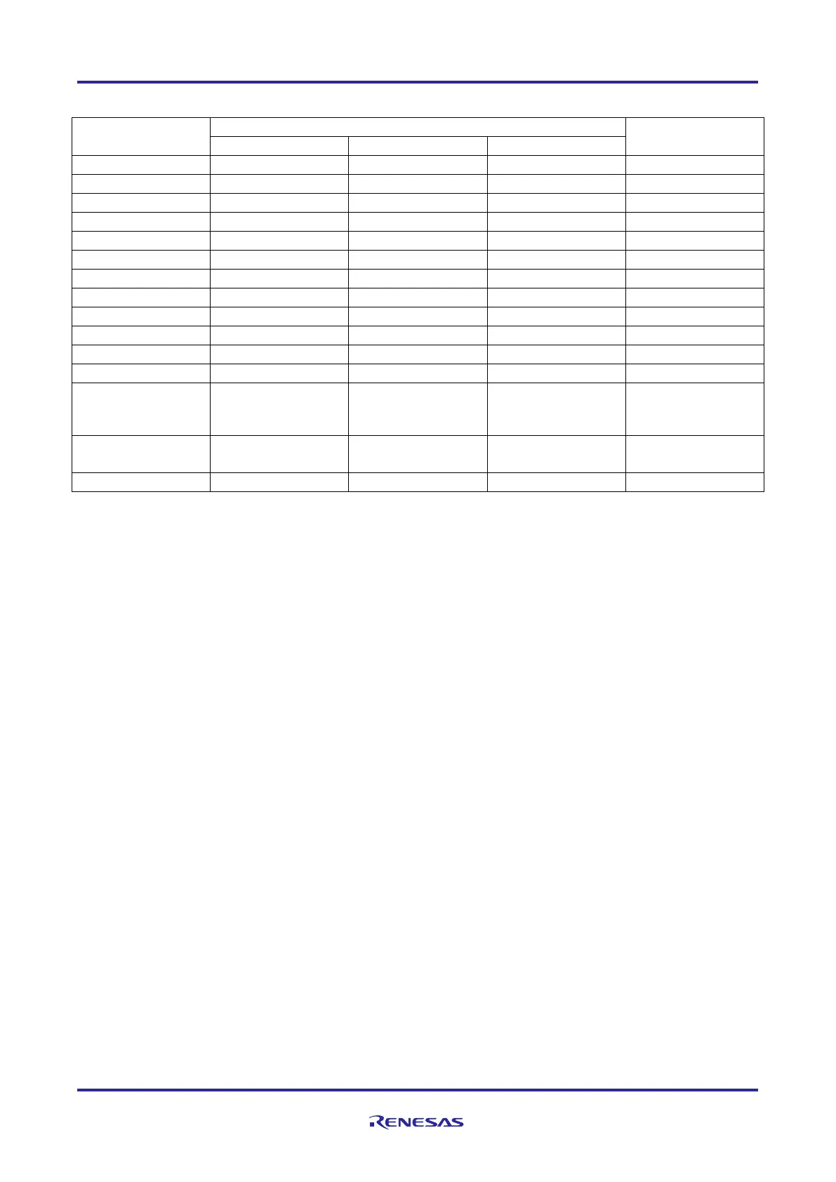
Table 8 Minimum external components for RH850/F1K (176pin)
C5, C6, C7, C8,
C10, C11, C12,
C14
The shown values for reference only.
The final values must be evaluated (with the resonator manufacturer).
The shown values are for reference only.
It must be ensured (by the schematic/PCB designer) that the voltage levels at the device pins always
remain within the specified range of the electrical characteristics (described in the RH850/F1K hardware
user’s manual).
See chapter RESET for details.
For values much smaller than the typical values, the connected devices might not be able to apply a low
level to the signal. Additionally higher currents will flow through the resistor / device.
A low level must be applied to FLMD1 in case FLMD0 becomes ‘1’ for external flash programming.
As a minimum value, a direct connection to VSS can be applied. But in case the related port (P10_8) is
switched to output ‘1’, it will damage the port/device.
In case of smaller values than the min. value, the typically connected device (E1) is not able to apply a
high (‘1’) signal.
For values much higher than the typical value, the required signal timings might not be achieved due to
the weaker currents. Additionally environmental effects (e.g. moisture and dirt) might generate other
weak currents and therefore influence the signal.
See chapter Development and Test Tool Interface for details.
See chapter JP0_4/_DCUTRST and chapter Recommended Connection of Unused Pins for details.
The resistor is only required when the JTAG/Nexus interface is used for debugging and depends on the
specification of the 3
rd
party development tool specification. See chapter Development and Test Tool
Interface for details.
The definition of components categories is as follows:
• Required component
Component that must be implemented as part of the device specification.
 Loading...