RH850/F1K Series Hardware Design Guide
R01AN2911EJ0100 Rev. 1.00 Page 20 of 46
Aug 04, 2016
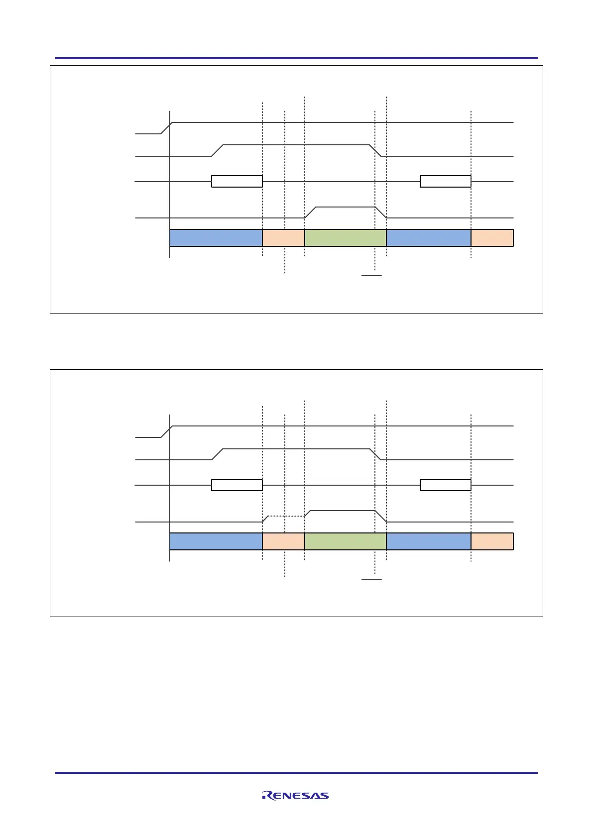
Figure 9 RESETOUT pin behavior at OPBT0[9] = 1
Figure 10 RESETOUT pin behavior at OPBT0[9] = 0
Caution
Until being disabled by register settings, the pin P8_6 drives an output low-level or high-z after any kind of reset.
To avoid a data collision, the outside circuit connected to the P8_6 pin must not drive high-level.
EVCC/REGVCC
RESET
P8_6
Execution of
user application
starts
P8_6 set to 1
RESET is
asserted
P8_6 changed to output
low level by any RESET
Flash operation
Flash sequence Flash sequence
RESETOUT I/O RESETOUT
RESETOUT
enable
RESETOUT
enable
Data transfer of
option byte
(OPBT0[9])
EVCC/REGVCC
RESET
P8_6
Execution of
user application
starts
P8_6 set to 1
RESET is
asserted
P8_6 changed to output
low level by any RESET
Flash operation
Flash sequence Flash sequence
RESETOUT I/O RESETOUT
RESETOUT
enable
RESETOUT
enable
Data transfer of
option byte
(OPBT0[9])
High-z
 Loading...