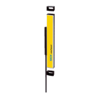
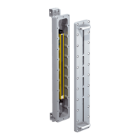
Table 30: Mechanical data
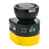
deTec4 C4P-EAxxx3SC05
Housing material Aluminum extruded profile
Front screen material PMMA
Table 31: Technical data for sender
Minimum Typical Maximum
Wavelength of sender Near-infrared
(NIR
), invisible
Weight Depending on the protective field height, see "Table of
weights", page 86
Laser alignment aid
Wavelength 650nm (red)
Average output power 390µW
Laser class 1
Laser alignment aid switch input (In1)
Input voltage HIGH (active) 13V 24V 30V
Input current HIGH 2mA 5mA 7mA
Input voltage LOW (deactivated) -3V 0V 3V
Input current LOW -0.1mA 0mA 0.5mA
Laser alignment aid pushbutton input (In2)
Input voltage HIGH (active) 13V 24V 30V
Input current HIGH 2mA 5mA 7mA
Input voltage LOW (deactivated) -3V 0V 3V
Input current LOW -0.1mA 0mA 0.5mA
Control switch actuation time 50ms
Permissible cable resistance
1)
Supply cable
2)
2.5Ω
1)
Limit the individual conductor resistance to the specified values to ensure that the light curtain functions
cor
rectly. (Also observe IEC60204-1.)
The specified values apply to the total resistance of each wire including contact and connector resistan‐
ces.
2)
If a T-connector is used, the specified values apply to the resistance of the entire cable from the system
connection of the device to the connection in the control cabinet.
Table 32: Technical data for receiver
Minimum Typical Maximum
Output signal switching devices
(OS
SDs)
2 PNP semiconductors, short-circuit protected
1)
, cross-
circuit monitored
Response time "Response time", page 84
Duration of OFF state 100ms
Switch-on delay 3 × response
t
ime
ON state, switching voltage HIGH
(U
rms
)
2)
U
V
– 2.25V 24V U
V
OFF state, switching voltage LOW
2)
3)
0V 0V 2.0V
Current-carrying capacity of the
O
SSDs
500mA each
Leakage current of the OSSDs 2mA each
13 TECHNICAL DATA
82
O P E R A T I N G I N S T R U C T I O N S | deTec4 C4P-EAxxx3SC05 8028570/2023-07-27 | SICK
Subject to change without notice

 Loading...