3.1 Mounting and Connections
375
7SA522 Manual
C53000-G1176-C155-3
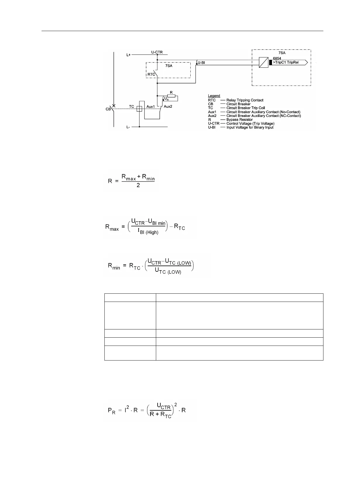
Figure 3-2 Trip circuit supervision with one binary input — Example for trip circuit 1
This results in an upper limit for the resistance dimension, R
max
, and a lower limit R
min
,
from which the optimal value of the arithmetic mean R should be selected:
In order that the minimum voltage for controlling the binary input is ensured, R
max
is
derived as:
To keep the circuit breaker trip coil energized in the above case, R
min
is derived as:
If the calculation yields that R
max
R
min
, the calculation must be repeated using the next
lowest switching threshold U
BI min
, and this threshold must be implemented in the relay
using plug-in jumpers (see Section “Hardware Modifications”).
For the power consumption of the resistance:
I
BI (HIGH)
Constant current with activated BI ( = 1.8 mA)
U
BImin
Minimum control voltage for BI (19 V for delivery setting for nominal volt-
ages of 24/48/60 V; 88 V for delivery setting for nominal voltages of
110/125/220/250 V, 176 V for delivery setting for nominal voltages of
220/250 V)
U
CTR
Control voltage for trip circuit
R
TC
DC resistance of circuit breaker trip coil
U
TC (LOW)
Maximum voltage on the circuit breaker trip coil that does not lead to trip-
ping
 Loading...