105
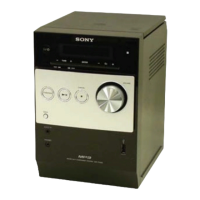
HCD-FL5D
• MC BOARD IC101 M30622MGN-B06FP (SYSTEM CONTROLLER)
Pin No. Pin Name I/O Description
1AMP-DATA O
Serial data output to the M61520FP
2AMP-CLK O
Serial data transfer clock signal output to the M61520FP
3AMP-LAT O
Serial data latch pulse signal output to the M61520FP
4 SIRCS I
Remote control signal input from the remote control receiver
5 DIG-TX O
Serial data output to the audio digital signal processor and digital audio interface receiver
6 DSP-RX
I Serial data input from the digital audio interface receiver
7 DIG-CLK
O
Serial data transfer clock signal output to the audio digital signal processor and
digital audio interface receiver
8 GND —
Ground terminal
9 GND —
Not used
10 XC-IN I
Sub system clock input terminal (32.768 kHz)
11 XC-OUT O
Sub system clock output terminal (32.768 kHz)
12 RESET I
System reset signal input from the reset signal generator “L”: reset
For several hundreds msec. after the power supply rises, “L” is input, then it changes to “H”
13 XOUT O
Main system clock output terminal (16 MHz)
14 VSS —
Ground terminal
15 XIN I
Main system clock input terminal (16 MHz)
16 VCC —
Power supply terminal (+3.3V)
17 NMI I
Non-maskable interrupt input terminal Fixed at “H” in this set
18 RDS-INT
I Serial data transfer clock signal input terminal Not used
19 SCOR
I Subcode sync (S0+S1) detection signal input terminal Not used
20 DIR-INT O
Interrupt request signal output to the digital audio interface receiver
21 CAPM-H/L O
High/normal speed selection signal output of the capstan motor
“L”: high speed, “H”: normal speed
22 CAPM-CNT1 O
Capstan motor drive signal output
23 A TRG O
Deck-A side trigger plunger drive signal output “H”: plunger on
24 BU-PWM3 O
RFDC PWM signal output terminal Not used
25 B TRG O
Deck-B side trigger plunger drive signal output “H”: plunger on
26 BU-PWM2 O
PWM signal output terminal Not used
27 A-HALF I
Deck-A cassette detection signal input terminal “L”: no cassette, “H”: cassette in
28 BU-PWM1 O
Focus servo drive PWM signal output terminal Not used
29 IIC-CLK I/O
IIC data reading clock signal input or transfer clock signal output with the fuluorescent indicator
driver and DVD system processor
30 IIC-DATA I/O
IIC two-way data bus with the fuluorescent indicator driver
31
CAN'T USE I Not used
32
SQ-DATA-IN I Subcode Q data input terminal Not used
33
SQ-CLK O Subcode Q data reading clock signal output terminal Not used
34
SENS I Internal status detection monitor input terminal Not used
35
CD-DATA
O
Serial data output terminal Not used
36
CAN'T USE I Not used
37 CD-CLK O
Serial data transfer clock signal output terminal Not used
38 POWER LED O
LED drive signal output terminal
39 CLOCK-OUT O
Clock (32.768 kHz) signal output terminal (for test mode) Not used
40
LDON(3STATE)
O
Laser diode on/off control signal output terminal Not used
41 M-RESET I
Reset signal output to the fluorescent indicator tube driver and front panel controller