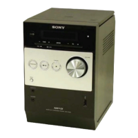
HCD-FL5D
4343
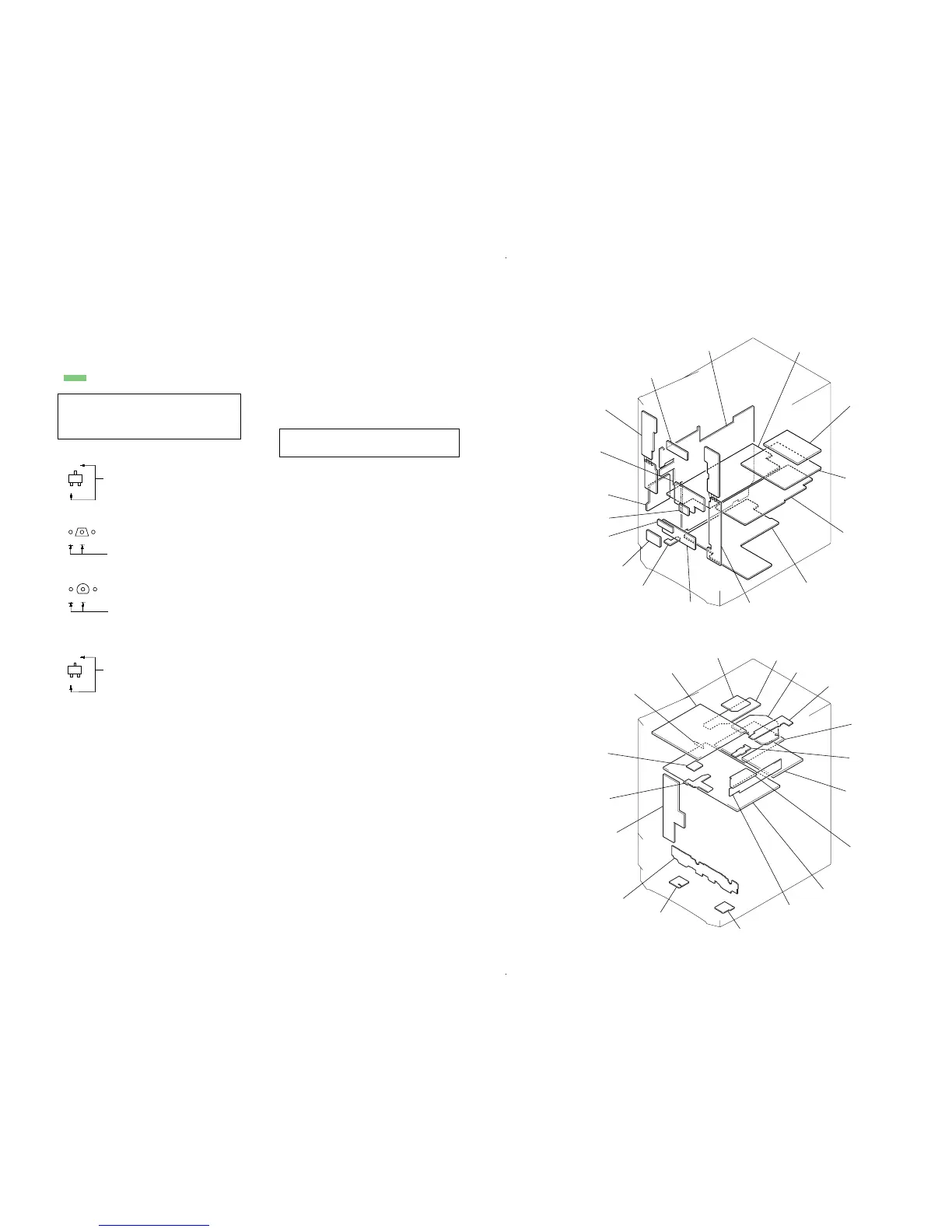
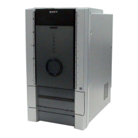
8-7. NOTE FOR PRINTED WIRING BOARDS AND SCHEMATIC DIAGRAMS
Note on Printed Wiring Boards:
• X : parts extracted from the component side.
• Y : parts extracted from the conductor side.
•
f
: internal component.
• : Pattern from the side which enables seeing.
(The other layers' patterns are not indicated.)
• Indication of transistor.
C
B
These are omitted.
E
Q
B
These are omitted.
CE
Q
B
These are omitted.
CE
Q
Note on Schematic Diagram:
• All capacitors are in µF unless otherwise noted. pF: µµF
50 WV or less are not indicated except for electrolytics
and tantalums.
• All resistors are in Ω and
1
/
4
W or less unless otherwise
specified.
•
f
: internal component.
• 2 : nonflammable resistor.
• 5 : fusible resistor.
• C : panel designation.
• A : B+ Line.
• B : B– Line.
• H : adjustment for repair.
•Voltages are taken with a VOM (Input impedance 10 MΩ).
Voltage variations may be noted due to normal produc-
tion tolerances.
•Waveforms are taken with a oscilloscope.
Voltage variations may be noted due to normal produc-
tion tolerances.
• Circled numbers refer to waveforms.
• Signal path.
F : AUDIO
L : VIDEO
E : Y
a : CHROMA
r : COMPONENT VIDEO
f : TUNER
E : TAPE PLAY (DECK A)
d : TAPE PLAY (DECK B)
G : REC (DECK B)
J : CD PLAY
c : DVD PLAY
N : MIC
j : MD (VIDEO)
i : OPTICAL DIGITAL IN
•Abbreviation
AUS: Australian model
EA : Saudi Arabia model
MX : Mexican model
SP : Singapore model
TH : Thai model
• Circuit Boards Location
Caution:
Pattern face side: Parts on the pattern face side seen from
(Conductor Side) the pattern face are indicated.
Parts face side: Parts on the parts face side seen from
(Component Side) the parts face are indicated.
D
G
These are omitted.
S
Q
Note: The components identified by mark 0 or dotted line
with mark 0 are critical for safety.
Replace only with part number specified.
SP relay board
video board
SUB TRANS boar