HCD-FL5D
8989
JW922
JW923
CN915
CN916
CN914
T911
NO3
R912
D911
R914
Q971
R915
R916R917
C915
D913 D912
D914 C914
R913
C913
JW928
F915
F919
JW921
6P
8P
7P
11ES2N
-TB5
1k
2SA1932
10k
100100
100
50V
RD6.2F
-T7B2
MTZJ-T-72
-39A
MTZJ-T-72
-3.6A
1
50V
0.68
100
63V
T8AL
250V
T5AL
250V
∗
D-GND
VP
VF
VF
AC2(VH)
AC2(VH)
AC1(VL)
AC1(VL)
AC3(MOTOR)
AC3(MOTOR)
AC4(PRE)
AC4(PRE)
AC2(VH)
AC2(VH)
AC1(VL)
AC1(VL)
N.C.
AC GND
AC GND
AC GND
AC GND
-42V
REGULATOR
TRANSFORMER
POWER
MAIN
230/240
220
120
NEURAL
2P
4P
∗
NO3
D911
RECT
(EXCEPT EA,SP)
(EA,SP)
(EA,SP)
(EXCEPT EA,SP)
(EA,MX,SP)
(TH)
(AUS)
F914
T8AL
250V
F916
T8AL
250V
F918
T6.3AL
250V
F917
T8AL
250V
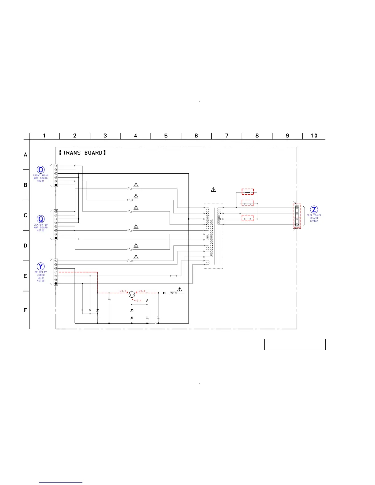
8-51. SCHEMATIC DIAGRAM – TRANS Board –
The components identified by mark 0 or dotted
line with mark 0 are critical for safety.
Replace only with part number specified.
•Voltages and waveforms are dc with respect to ground
under no-signal (detuned) conditions.
no mark : TUNER
(Page 73)
(Page 71)
(Page 77)
(Page 87)