113
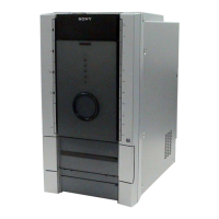
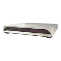
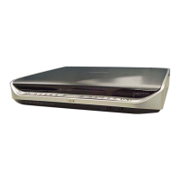
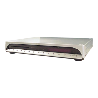
HCD-FL5D
• GC BOARD IC202 PT8300 (FRONT PANEL CONTROLLER)
Pin No. Pin Name I/O Description
1 VSS —
Ground terminal
2
RESET_B I Reset signal input from the system controller
3
CLK I Serial data transfer clock signal input from the fuluorescent indicator driver
4
LATCH I Serial data latch pulse input from the fuluorescent indicator driver
5
TC SW I Key input terminal (A/D input)
6
CD SW 3 I Key input terminal (A/D input)
7
CD SW 2 I Key input terminal (A/D input)
8
CD SW 1 I Key input terminal (A/D input)
9
H.P I Headphone detection signal input
10 to 12
NC O Not used
13
LATCHO O Serial data latch pulse output terminal
14
CLKO O Serial data transfer clock signal output terminal
15
DO1 O Serial data output terminal Not used
16
DI2 I Serial data input terminal Not used
17
TC A SW O TC holder open plunger drive signal output (DECK A)
18
TC B SW O TC holder open plunger drive signal output (DECK B)
19 to 23
LED5 to LED1 O LED drive signal output terminal
24
LED SELECT O LED drive signal output terminal
25
DO2 O Serial data output to the fuluorescent indicator driver
26
DO1 I Serial data input from the fuluorescent indicator driver
27
PULLDO — Not used
28 VCC
— Power supply terminal (+3.3V)