When using the external debug connectors (CN12 or CN18), the STLINK-V3EC can be used to supply the
STM32H573I-DK board through CN10 USB Type-C
®
connector. Otherwise, another power supply source can be
used as described on Section 9 Power supply.
Two level shifters are used on VCP and SWD interfaces to offer a debug capability when operating the target
MCU at 1.8 V. The level shifters are used to allow compatibility between target MCU signals (1V8 or 3V3) and
STLINK-V3EC signals (3V3).
The U26 level shifter is disabled with the JP1 jumper to isolate the output I/Os from STLINK-V3EC when an
external debug tool is used. The configuration of the JP1 jumper is explained in Table 15. JP1 jumper settings.
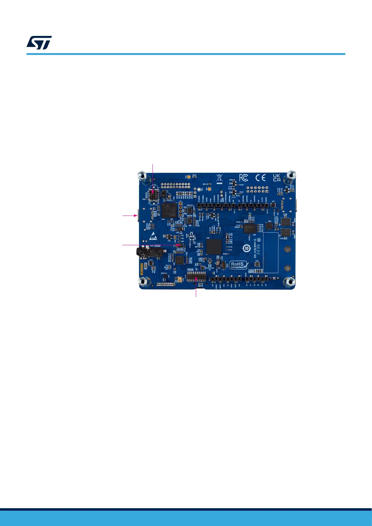
Figure 7. Connecting an external debug tool to program the on-board STM32
DT71727V1
MIPI-10 connector (CN12)
(SWD/JTAG)
STLINK-V3EC USB
connector (CN10)
External debugger
selection (JP1)
MIPI-20 connector (CN18)
(trace)
UM3143
Using an external debug tool to program and debug the on-board STM32
UM3143 - Rev 1
page 12/53

 Loading...


