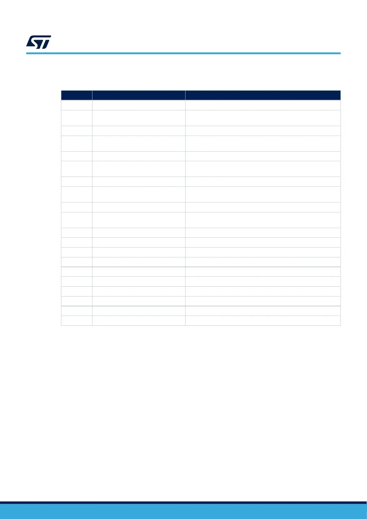
Table 5 describes the MIPI20 connector pinout (CN18).
Table 5. MIPI20 debug connector pinout (CN18)
MIPI20 pin CN18 Designation
1 VCC Target VCC
2 SWDIO/JTMS
Target SWDIO using SWD protocol or target JTMS using JTAG
protocol
3 GND Ground
4 SWCLK/JCLK
Target SWCLK using SWD protocol or target JCLK using JTAG
protocol
5 GND Ground
6 JTDO/SWO
Target SWO using SWD protocol or target JTDO using JTAG
protocol
7 KEY Not connected
8 JTDI
Not used by SWD protocol, target JTDI (T_JTDI) using JTAG
protocol, only for external tools
9 GND Ground
10 NRST
Target NRST using SWD protocol or target JTMS (T_JTMS) using
JTAG protocol
11 TgtPwr 5 V target power to the target MCU – To be disconnected
12 TRACECLK Trace clock
13 TgtPwr 5V target power to the target MCU – To be disconnected
14 TRACED0 Trace Data0
15 GND Ground
16 TRACED1 Trace Data1
17 GND Ground
18 TRACED2 Trace Data2
19 GND Ground
20 TRACED3 Trace Data3
UM3143
Using an external debug tool to program and debug the on-board STM32
UM3143 - Rev 1
page 14/53

 Loading...


