Theory of Operation-2445A/2455A Service
Address Decode
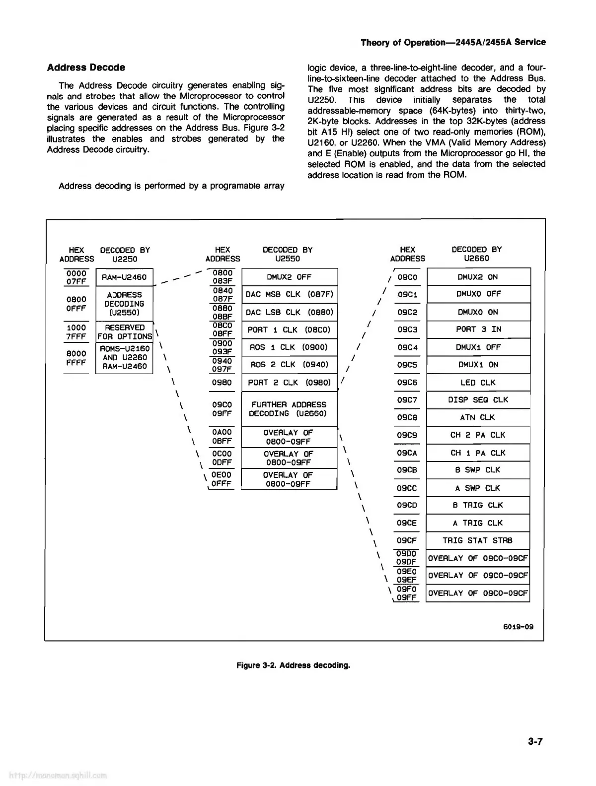
The
Address Decode circuitry generates enabling sig-
nals
and
strobes that allow the Microprocessor to control
the various devices
and
circuit functions.
The
controlling
signals
are
generated
as
a result of the Microprocessor
placing specific addresses
on
the Address Bus.
Figure
3-2
illustrates the enables
and
strobes generated
by
the
Address Decode circuitry.
logic device, a three-line-to-eight-line decoder,
and
a four-
line-to-sixteen-line decoder attached to the Address Bus.
The
five most significant address bits are decoded by
U2250. This device initially separates the total
addressable-memory space (64K-bytes) into thirty-two,
2K-byte blocks. Addresses
in
the top 32K-bytes (address
bit A15
HI)
select one of two read-0nly memories (ROM),
U2160, or U2260.
When
the VMA (Valid Memory Address)
and
E (Enable) outputs from the Microprocessor go
HI,
the
selected
ROM
is
enabled,
and
the data from the selected
address location
is
read
from the
ROM.
Address decoding
is
performed by a programaoIe array
HEX
ADDRESS
0000
07FF
0800
OFFF
1000
7FFF
8000
FFFF
DECODED
BY
U2250
RAM-U2460
ADDRESS
DECODING
(U2550)
RESERVED
FOR
OPTIONS
ROMS-U2160
AND
U2260
RAM-U2460
I o
\
\
\
\
\
\
\
HEX
ADDRESS
0800
083F
0840
087F
0880
08BF
OSCO
OBFF
0900
093F
0940
097F
\
0980
09CO
09FF
OAOO
\
OBFF
\
ocoo
ODFF
OEOO
OFFF
DECODED
BY
U2550
DMUX2
OFF
DAC
MSB
CLK
(087F)
DAC
LSB
CLK
(0880)
PORT
1
CLK
(OSCO)
ROS
1
CLK
(0900)
ROS
2
CLK
(0940)
PORT
2
CLK
(0980)
FURTHER
ADDRESS
DECODING
(U2660)
OVERLAY
OF
0800-09FF
OVERLAY
OF
0800-09FF
OVERLAY
OF
0800-09FF
I
I
\
\
\
Figure 3-2. Address decoding.
I
I
\
\
\
I
I
I
\
\
\
\
HEX
ADDRESS
09CO
09C1
I
09C2
09C3
09C4
09C5
09C6
09C7
09C8
09C9
09CA
09CB
09CC
09CD
09CE
09CF
\
09DO
\
09DF
09EO
\
09EF
\
09FO
1
09FF
DECODED
BY
U2660
DMUX2
ON
DMUXO
OFF
DMUXO
ON
PORT
3
IN
DMUX1
OFF
DMUX1
ON
LED
CLK
DISP
SEQ
CLK
ATN
CLK
CH
2
PA
CLK
CH
1
PA
CLK
B
SWP
CLK
A
SWP
CLK
B
TRIG
CLK
A
TRIG
CLK
TRIG
STAT
STAB
OVERLAY
OF
09C0-09CF
OVERLAY
OF
09C0-09CF
OVERLAY
OF
09C0-09CF
6019-09
3-7