Theory
of
Operation-2445A/2455A Service
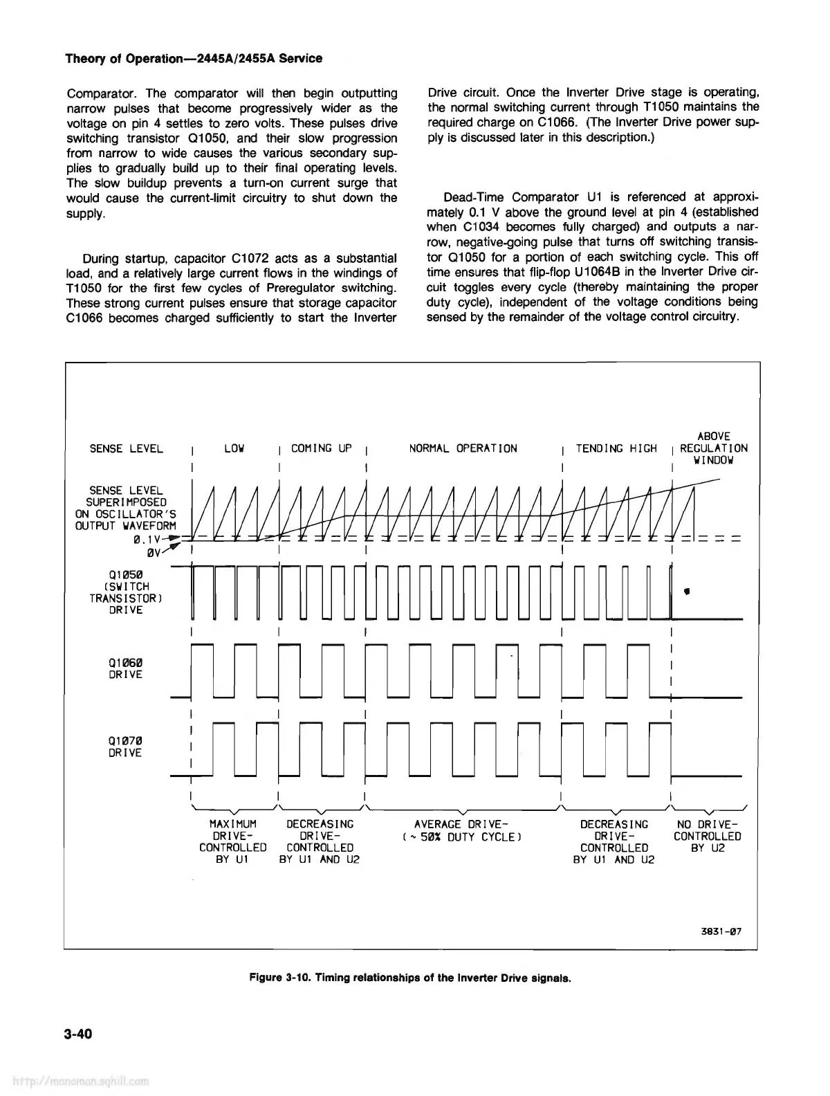
Comparator.
The
comparator will
then
begin
outputting
narrow pulses that
become
progressively wider
as
the
voltage
on
pin
4 settles to zero volts. These pulses drive
switching transistor 01050,
and
their slow progression
from narrow to wide causes the various secondary sup-
plies to gradually build
up
to their final operating levels.
The slow buildup prevents a turn-on current surge that
would cause the current-limit circuitry to shut down the
supply.
During startup, capacitor C1072 acts as a substantial
load,
and
a relatively large current flows
in
the windings of
T1050 for the first few cycles of Preregulator switching.
These strong current pulses ensure that storage capacitor
C1066 becomes charged sufficiently to start the Inverter
SENSE
LEVEL
SENSE
LEVEL
SUPERIMPOSED
ON
OSCILLATOR'S
OUTPUT
WAVEFORM
0.1V
0V
01050
(SWITCH
TRANSISTOR)
DRIVE
01060
DRIVE
01070
DRIVE
LOW
COMING
UP
Drive circuit.
Once
the Inverter Drive stage is operating,
the normal switching current through T1050 maintains the
required charge
on
C1066. (The Inverter Drive power sup-
ply
is
discussed later
in
this description.)
Dead-Time Comparator U 1 is referenced at approxi-
mately
0.1
V above the ground
level
at
pin
4 (established
when C1034 becomes fully charged)
and
outputs a nar-
row, negative-going pulse that turns off switching transis-
tor 01050 for a portion of
each
switching cycle. This off
time ensures that flip-flop U1064B
in
the Inverter Drive cir-
cuit toggles every cycle (thereby maintaining the proper
duty
cycle),
independent of the voltage conditions
being
sensed
by
the remainder of the voltage control circuitry.
NORMAL
OPERATION
ABOVE
TENDING
HIGH
REGULATION
WINDOW
I I I I
MAX
I
MUM
DECREASING
AVERAGE
DR
I
VE-
DECREASING
ND
DR
I
VE
DR
I
VE-
DR
I
VE-
(
DUTY
CYCLE
J
DR
I
VE
CONTROLLED
CONTROLLED
CONTROLLED
CONTROLLED
BY
U2
BY
Ul
BY
Ul
AND
U2
BY
Ul
AND
U2
Figure 3-10. Timing relationships of the Inverter Drive signals.
3-40