7 Series FPGAs GTP Transceivers User Guide www.xilinx.com 185
UG482 (v1.9) December 19, 2016
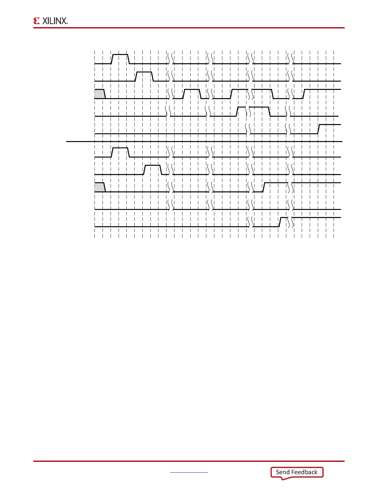
RX Buffer Bypass
Notes relevant to Figure 4-42:
1. The sequence of events shown in Figure 4-42 is not drawn to scale.
2. M_* denotes ports related to the master lane.
3. S_* denotes ports related to the slave lane(s).
4. After conditions such as a GTP receiver reset or RX rate change, RX phase alignment must be
performed to align XCLK and RXUSRCLK. Wait until exiting RXELECIDLE and RX CDR is
locked before asserting RXDLYSRESET to start the RX phase and delay alignments. The
assertion of RXDLYSRESET should be less than 50 ns.
5. Wait until RXDLYSRESETDONE is High. RXDLYSRESETDONE will stay asserted for a
minimum of 100 ns.
6. When RXSYNCDONE of the master lane is asserted, the alignment procedure is completed.
This signal will remain asserted until alignment procedure is re-initiated.
7. Upon the assertion of RXSYNCDONE of the master lane, RXPHALIGNDONE of the master
lane indicates whether alignment is achieved and maintained.
8. RX delay alignment continues to adjust RXUSRCLK to compensate for temperature and
voltage variations.
In a multi-lane application, it is necessary to start the RX alignment procedure on the interface after
RXELECIDLE is deasserted on any lane. RX CDR of all lanes needs to be locked before starting the
RX alignment procedure. This requirement is to make sure the RX recovered clocks and
RXUSRCLK are stable and ready before alignment.
X-Ref Target - Figure 4-42
Figure 4-42: RX Buffer Bypass Example—Multi-Lane Auto Mode
M_RXDLYSRESET
M_RXDLYSRESETDONE
M_RXPHALIGNDONE
M_RXSYNCOUT
M_RXSYNCDONE
S_RXDLYSRESET
S_RXDLYSRESETDONE
S_RXPHALIGNDONE
S_RXSYNCOUT
S_RXSYNCDONE
UG482_c4_141_020613