EasyManua.ls Logo

Xilinx 7 Series User Manual

Xilinx 7 Series
306 pages
To Next Page IconTo Next Page
To Previous Page IconTo Previous Page
Page #212 background imageLoading...
Page #212 background image
212 www.xilinx.com 7 Series FPGAs GTP Transceivers User Guide
UG482 (v1.9) December 19, 2016
Chapter 4: Receiver
The state machine works by keeping track of valid and invalid synchronization headers. Upon reset,
block lock is deasserted, and the state is LOCK_INIT. The next state is RESET_CNT where all
counters are zeroed out. The synchronization header is analyzed in the TEST_SH state. If the header
is valid, sh_cnt is incremented in the VALID_SH state, otherwise sh_count and sh_invalid_count
are incremented in the INVALID_SH state.
For the block synchronization state machine shown in Figure 4-57, sh_cnt_max and
sh_invalid_cnt_max are both constants that are set to 64 and 16, respectively. From the VALID_SH
state, if sh_cnt is less than the value sh_cnt_max and test_sh is High, the next state is TEST_SH. If
sh_cnt is equal to sh_cnt_max and sh_invalid_cnt equals 0, the next state is GOOD_64 and from
there block_lock is asserted. Then the process repeats again and the counters are cleared to zeros. To
achieve block lock, the state machine must receive sh_cnt_max number of valid synchronization
headers in a row without getting an invalid synchronization header. However, when block lock is
achieved sh_invalid_cnt_max 1, the number of invalid synchronization headers can be received
within sh_cnt_max number of valid synchronization headers. Thus, once locked, it is harder to break
lock.
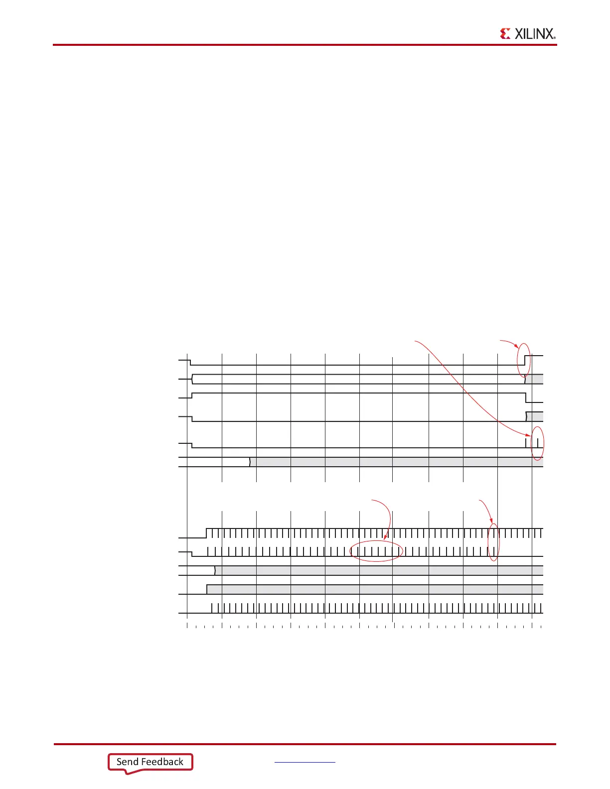
Figure 4-58 shows a waveform of the block synchronization state machine asserting
RXGEARBOXSLIP numerous times because of invalid synchronization headers before achieving
data alignment. After the RXGEARBOXSLIP is issued, the state machine waits
32 RXUSRCLK2 cycles before checking for valid synchronization headers.
X-Ref Target - Figure 4-58
Figure 4-58: RX Gearbox with Block Synchronization
UG482_c4_40_111011
Data alignment
achieved
Data check on
unscrambled data
block_sync_i
unscrambled_data_i
begin_r
track_data_r
start_of_packet_detected_r
RXDATA
RXDATAVALID
RXGEARBOXSLIP
RXHEADER
RXHEADERVALID
RXSTARTOFSEQ
0
Slip data
alignment
Closely spaced slip pulses. State machine
asserts slip as soon as it sees bad header.
0000000000000000
0000000000000000
Send Feedback

Table of Contents

Question and Answer IconNeed help?

Do you have a question about the Xilinx 7 Series and is the answer not in the manual?

Xilinx 7 Series Specifications

General IconGeneral
Process Technology28nm
TransceiversUp to 96
I/O PinsUp to 1, 200
Transceiver Data RateUp to 28.05 Gbps
Power ConsumptionVaries by device
Operating TemperatureCommercial, Industrial
Package OptionsBGA, CSP
FamilyArtix-7, Kintex-7, Virtex-7
DSP Slices16 - 3600

Summary

Chapter 1: Transceiver and Tool Overview

Overview and Features

Summary of GTP transceiver features and capabilities, including data rate and protocol support.

7 Series FPGAs Transceivers Wizard

Details on using the Wizard to generate GTP transceiver instantiation wrappers.

Simulation

Prerequisites and considerations for simulating GTP transceiver designs.

Implementation

Information on mapping GTP transceivers to device resources and creating UCF files.

Chapter 2: Shared Features

Reference Clock Input Structure

Description of the reference clock input buffer and its internal structure.

Reference Clock Selection and Distribution

Options for reference clock input, routing, and selection for GTP transceivers.

PLL

Details on the ring oscillator PLLs (PLL0 and PLL1) within the GTP Quad.

Reset and Initialization

Procedure for initializing the GTP transceiver after FPGA configuration.

Reset Modes

Explanation of sequential and single reset modes for GTP transceiver operation.

PLL Reset

Procedure for resetting the PLLs (PLL0 and PLL1) before use.

TX Initialization and Reset

Details on the TX reset state machine and its operation.

RX Initialization and Reset

Overview of RX initialization and reset processes, including sequential and single modes.

Power Down

Description of power-down modes for GTP transceiver channels and PLLs.

Loopback

Configuration and functionality of loopback modes for transceiver testing.

Dynamic Reconfiguration Port

Interface for dynamically changing parameters of GTPE2_CHANNEL and GTPE2_COMMON primitives.

Digital Monitor

Visibility into adaptation loops and convergence states for link optimization.

Chapter 3: Transmitter

TX Overview

Introduction to the GTP transceiver transmitter's functional blocks.

FPGA TX Interface

The FPGA's gateway to the TX datapath, including interface width and clocking.

TX 8B/10B Encoder

Functionality, bit/byte ordering, and K characters for 8B/10B encoding.

TX Gearbox

Support for 64B/66B and 64B/67B encoding for high-speed data protocols.

TX Buffer

Description of the TX buffer and phase alignment circuit for resolving clock domain differences.

TX Buffer Bypass

Advanced feature for adjusting phase difference and TX delay alignment.

TX Pattern Generator

Generation of PRBS and other test patterns for signal integrity testing.

TX Configurable Driver

Features of the TX driver, including voltage control, pre-emphasis, and termination.

TX Receiver Detect Support for PCI Express Designs

Feature for the transmitter to detect receiver presence on a link.

TX Out-of-Band Signaling

Support for OOB sequences in SATA/SAS and beaconing in PCI Express.

Chapter 4: Receiver

RX Overview

Introduction to the GTP transceiver receiver's functional blocks.

RX Analog Front End

Description of the RX analog front end buffer with configurable termination.

RX Out-of-Band Signaling

Support for OOB sequences in SATA/SAS and beaconing in PCI Express.

RX Equalizer

Power-efficient adaptive CTLE for compensating signal distortion.

RX CDR

Clock and data recovery circuit architecture and operation.

RX Fabric Clock Output Control

Control of serial and parallel clock dividers for the RX datapath.

RX Margin Analysis

Mechanism to measure and visualize receiver eye margin after equalization.

RX Polarity Control

Functionality to invert the polarity of incoming data.

RX Pattern Checker

Built-in PRBS checker for testing signal integrity.

RX Byte and Word Alignment

Process of aligning serial data to symbol boundaries for parallel data usage.

RX 8B/10B Decoder

Decoding of 8B/10B encoded data, including features and error handling.

RX Buffer Bypass

Advanced feature to bypass the RX elastic buffer for reduced latency.

RX Elastic Buffer

Functionality of the RX elastic buffer for resolving clock domain phase differences.

RX Clock Correction

Mechanism to bridge clock domain differences and prevent buffer overflow/underflow.

RX Channel Bonding

Feature to cancel skew between lanes by adjusting RX elastic buffer latency.

RX Gearbox

Support for 64B/66B and 64B/67B header and payload separation.

FPGA RX Interface

The FPGA's gateway to the RX datapath, including port widths and clocking.

Chapter 5: Board Design Guidelines

Overview

Introduction to implementing GTP transceiver designs on printed circuit boards.

Pin Description and Design Guidelines

Guidelines for routing GTP transceiver signals and managing SelectIO activity.

GTP Pin Descriptions

Detailed description of GTP Quad pins and their functions.

Termination Resistor Calibration Circuit

Description of the RCAL circuit for resistor calibration.

Analog Power Supply Pins

Discussion of MGTAVCC and MGTAVTT power planes and their organization.

Reference Clock

Selection criteria for reference clock sources and oscillators.

Power Supply and Filtering

Considerations for analog power supplies, regulators, and filtering.

PCB Design Checklist

A checklist for designing and reviewing GTP transceiver PCB schematics and layouts.

Appendix A: Placement Information by Package

CPG236 Package Placement Diagram

Placement diagram for the CPG236 package, showing GTP transceiver locations.

CSG325 Package Placement Diagram

Placement diagram for the CSG325 package, showing GTP transceiver locations.

CLG485 Package Placement Diagram

Placement diagram for the CLG485 package, showing GTP transceiver locations.

FGG484 Package Placement Diagram

Placement diagram for the FGG484 package, showing GTP transceiver locations.

FGG676 Package Placement Diagram

Placement diagram for the FGG676 package, showing GTP transceiver locations.

FBG484 Package Placement Diagram

Placement diagram for the FBG484 package, showing GTP transceiver locations.

SBG484 Package Placement Diagram

Placement diagram for the SBG484 package, showing GTP transceiver locations.

FFG1156 Package Placement Diagram

Placement diagram for the FFG1156 package, showing GTP transceiver locations.

Appendix B: Placement Information by Device

Appendix C: 8B/10B Valid Characters

Appendix D: DRP Address Map of the GTP Transceiver

Related product manuals