230 www.xilinx.com 7 Series FPGAs GTP Transceivers User Guide
UG482 (v1.9) December 19, 2016
Chapter 5: Board Design Guidelines
Printed Circuit Board
The decoupling capacitors on the printed circuit board play an important role in minimizing the
effects of power supply noise on the transceivers. By providing a low impedance between the power
and ground planes, the PCB decoupling capacitors provide isolation between GTP transceivers in
the package.
De-coupling capacitors provide two basic functions. They help to isolate one circuit from another,
and they provide isolation between the power supply source and the load circuit. By minimizing the
power-to-ground impedance, noise induced on the power supply by one circuit will not induce noise
on the power supply of another circuit that is sharing the same power supply. In this case, the
concern would be noise coupling between GTP transceivers in the same FPGA. Also, de-coupling
capacitors provide isolation between the power supply source and the load circuit.
Power Supply Decoupling Capacitors
For the Artix-7 FPGA GTP transceiver analog power supplies, the primary purpose of decoupling
capacitors is to reduce the amplitude of the noise from the power supply source and other circuits on
the PCB. The suggested filtering for the power supplies, MGTAVCC and MGTAVTT, is provided in
Table 5-7.
Power Supply Decoupling Capacitor Layout and Placement
The effectiveness of the decoupling capacitors is directly dependent on their placement and routing
on the printed circuit board. The inductance of the path between the capacitors and the power and
ground planes on the die must be kept to a minimum. The lower the inductance in the path, the lower
the voltage noise generated by transient load currents.
The larger 4.7 µF capacitors should be placed in close proximity and outside the perimeter of the
FPGA pin field.
The 0.1µF capacitors on the other hand must be placed as close to the GTP Quad power supply pins
as possible. Placing the capacitors on the bottom of the board under the FPGA meets this
requirement. A couple of options are available for placing these capacitors.
One option is to use filled vias with an 0402 size capacitor. A capacitor of this size fits between the
vias. The via hole needs to be filled to keep the solder from wicking into the via. See Figure 5-10 for
an example of placement and routing of the 0.1 µF capacitors.
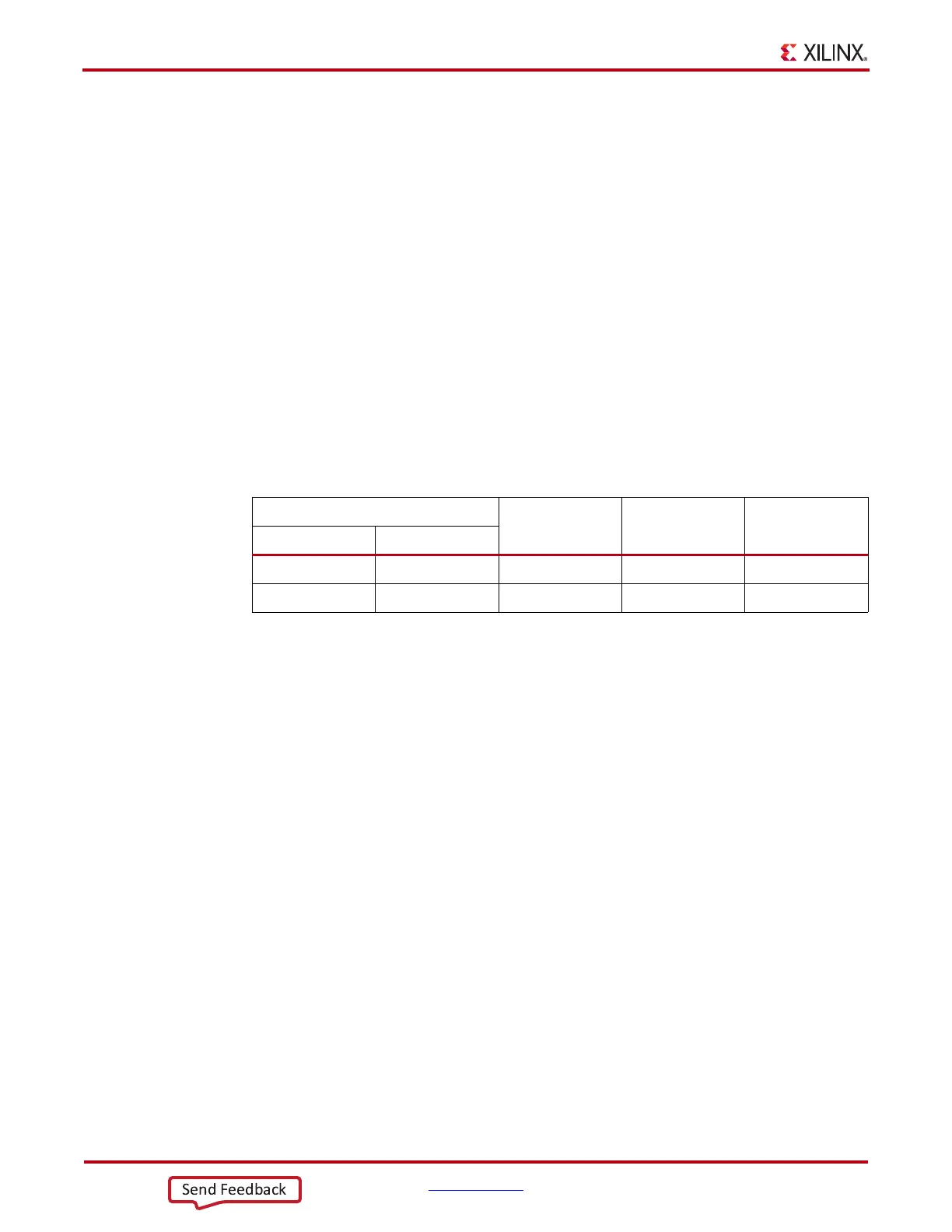
Table 5-7: Power Supply Filter Capacitor Recommendations
Qty/Power Supply Group
Capacitance
(µF)
Tolerance Type
MGTAVCC MGTAVTT
1 1 4.7 10% Ceramic
2 2 0.1 10% Ceramic
 Loading...


