EasyManuals Logo

Xilinx 7 Series User Manual

Xilinx 7 Series
306 pages
To Next Page IconTo Next Page
To Previous Page IconTo Previous Page
Page #231 background imageLoading...
Page #231 background image
7 Series FPGAs GTP Transceivers User Guide www.xilinx.com 231
UG482 (v1.9) December 19, 2016
Power Supply and Filtering
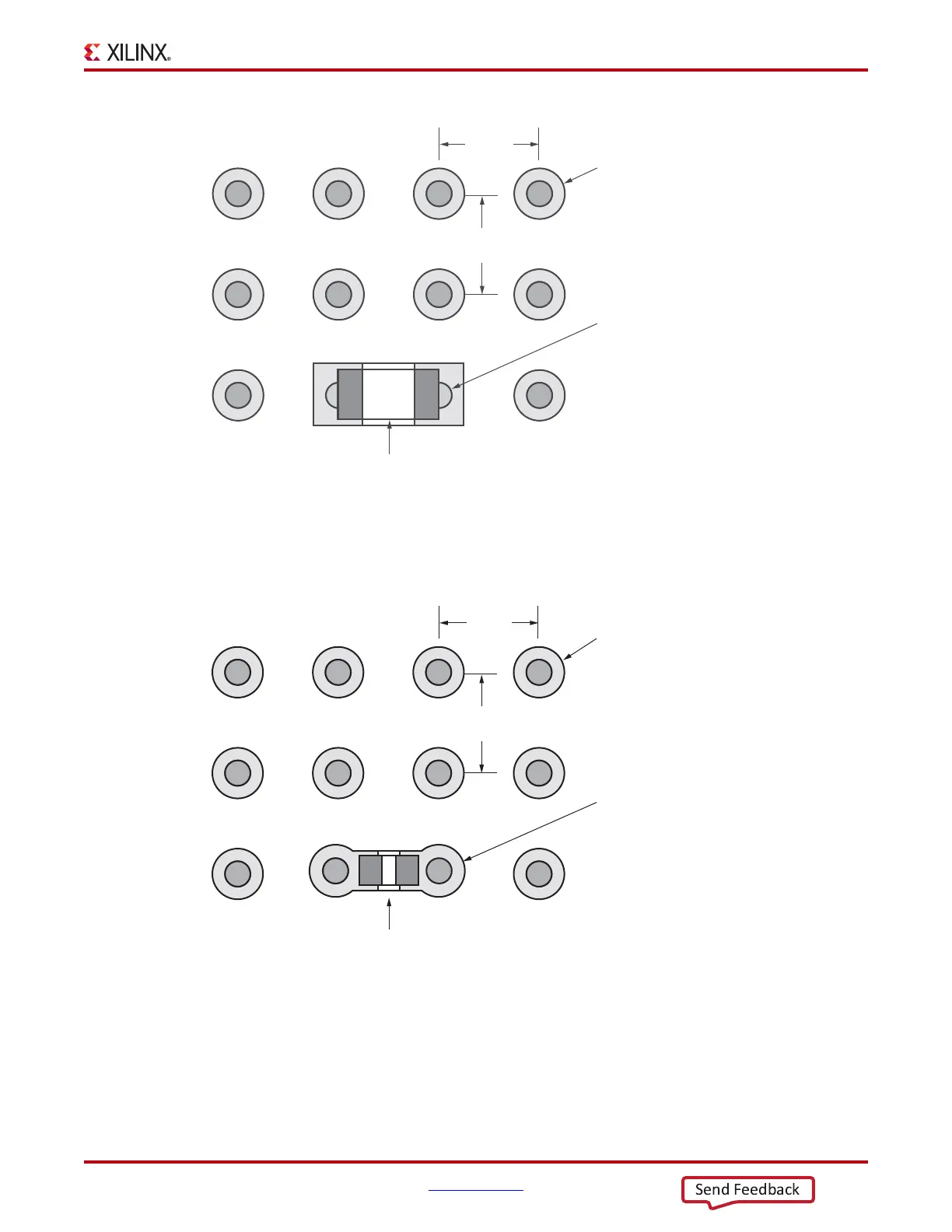
Another option is to use an 0201 capacitor and mounting it between the vias. An example of this is
shown in Figure 5-11.
X-Ref Target - Figure 5-10
Figure 5-10: Placement of 0.1 µF 0402 Capacitor Using Filled Via in Pad Under FPGA
1 mm.
BGA Pin Field Vias
Filled Via in Pad
0402 Capacitor
1 mm.View From Bottom of PCB
UG482_c5_10_072412
X-Ref Target - Figure 5-11
Figure 5-11: Placement of 0.1 µF 0201 Capacitor Using Filled Via in Pad Under FPGA
1 mm.
BGA Pin Field Vias
Filled Via in Pad
0201 Capacitor
1 mm.View From Bottom of PCB
UG482_c5_11_072412
Send Feedback

Table of Contents

Questions and Answers:

Question and Answer IconNeed help?

Do you have a question about the Xilinx 7 Series and is the answer not in the manual?

Xilinx 7 Series Specifications

General IconGeneral
Process Technology28nm
TransceiversUp to 96
I/O PinsUp to 1, 200
Transceiver Data RateUp to 28.05 Gbps
Power ConsumptionVaries by device
Operating TemperatureCommercial, Industrial
Package OptionsBGA, CSP
FamilyArtix-7, Kintex-7, Virtex-7
DSP Slices16 - 3600

Related product manuals