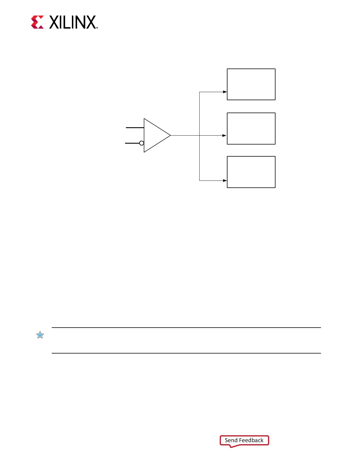
Figure 8: Single External Reference Clock with Multiple Duals
GTM_DUAL
GTREFCLK
MGTREFCLKP
MGTREFCLKN
I
IB
IBUFDS_GTM
O
GTM_DUAL
GTREFCLK
GTM_DUAL
GTREFCLK
D(n+1)
D(n)
D(n-1)
X20215-061418
Note: The IBUFDS_GTM diagram in the above gure is a simplicaon. The output port ODIV2 is le
oang, and the input port CEB is set to logic 0.
These rules must be observed when sharing a reference clock to ensure that jier margins for
high-speed designs are met:
• The number of Duals above the sourcing Dual must not exceed one.
• The number of Duals below the sourcing Dual must not exceed one.
• The total number of Duals sourced by an external clock pin pair (MGTREFCLKP/
MGTREFCLKN) must not exceed three Duals.
The maximum number of Duals that can be sourced by a single clock pin pair is three (six
transceivers). Designs with more than three Duals require the use of mulple external clock pins
to ensure that the rules for controlling jier are followed. When mulple clock pins are used, an
external buer can be used to drive them from the same oscillator.
IMPORTANT
! Upon device conguraon, the clock output from the IBUFDS_GTM which takes inputs
from MGTREFCLKP and MGTREFCLKN can only be used as long as the GTPOWERGOOD signal has
already asserted High.
Ports and Attributes
The following table denes the clocking ports and aributes for the GTM_DUAL primive.
Chapter 2: Shared Features
UG581 (v1.0) January 4, 2019 www.xilinx.com
Virtex UltraScale+ GTM Transceivers 17
 Loading...

