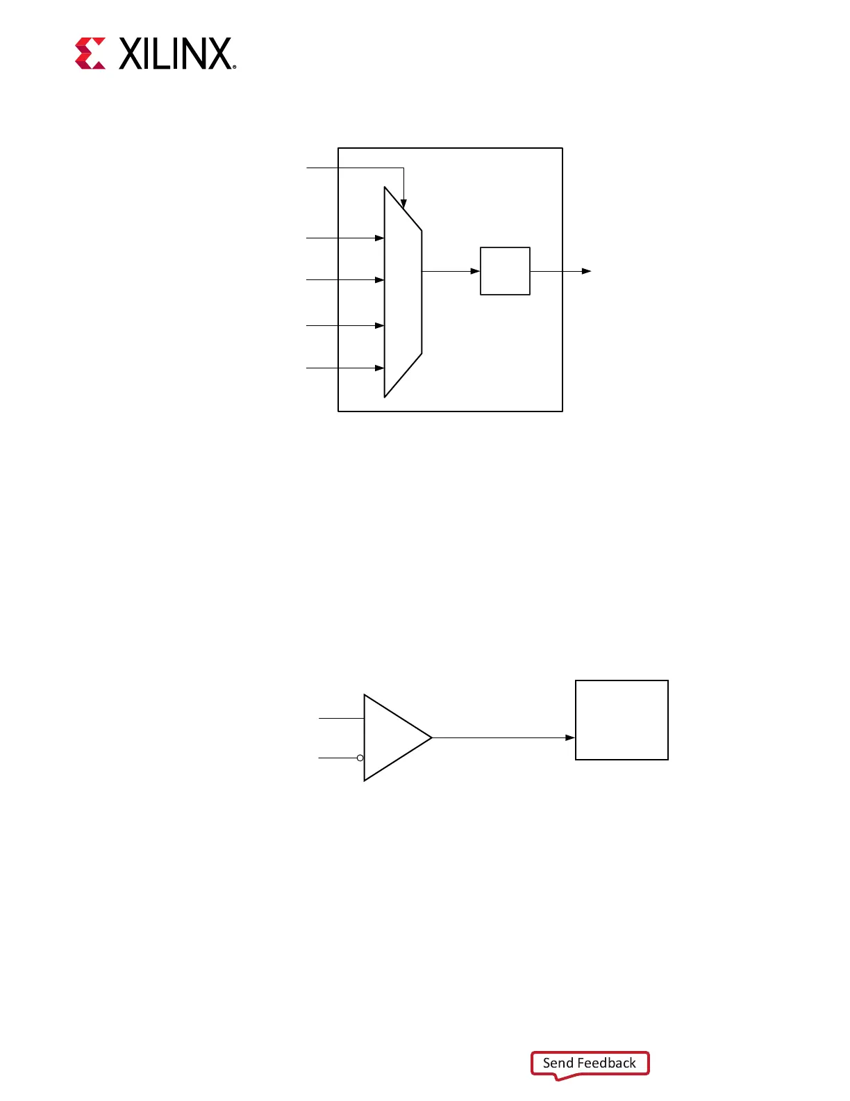
Figure 6: LCPLL Reference Clock Selection Multiplexer
LCPLL
0
1
2
3
4
5
6
7
GTREFCLK
GTNORTHREFCLK
LCPLL Output CLK
GTM_DUAL
PLLREFCLKSEL
GTSOUTHREFCLK
GTGREFCLK2PLL
X20897-061418
Single External Reference Clock Use Model
Each Dual has one set of dedicated dierenal reference clock input pins (MGTREFCLK[P/N])
that can be connected to the external clock sources. In a single external reference clock use
model, an IBUFDS_GTM must be instanated to use the dedicated dierenal reference clock
source. The following gure shows a single external reference clock connected to the LCPLL
inside the Dual. The user design connects the IBUFDS_GTM output (O) to the GTREFCLK ports
of GTM_DUAL.
Figure 7: Single External Reference Clock in a Dual
GTM_DUAL
GTREFCLK
MGTREFCLKP
MGTREFCLKN
I
IB
IBUFDS_GTM
O
X20898-061418
Note: The IBUFDS_GTM diagram in the above gure is a simplicaon. The output port ODIV2 is le
oang, and the input port CEB is set to logic 0.
The following gure shows a single external reference clock with mulple Duals connected. The
user design connects the IBUFDS_GTM output (O) to the GTREFCLK ports of the GTM_DUAL
primives. In this case, the Xilinx implementaon tools make the necessary adjustments to the
north/south roung as well as the pin swapping necessary to route the reference clock from one
Dual to another when required.
Chapter 2: Shared Features
UG581 (v1.0) January 4, 2019 www.xilinx.com
Virtex UltraScale+ GTM Transceivers 16
 Loading...

