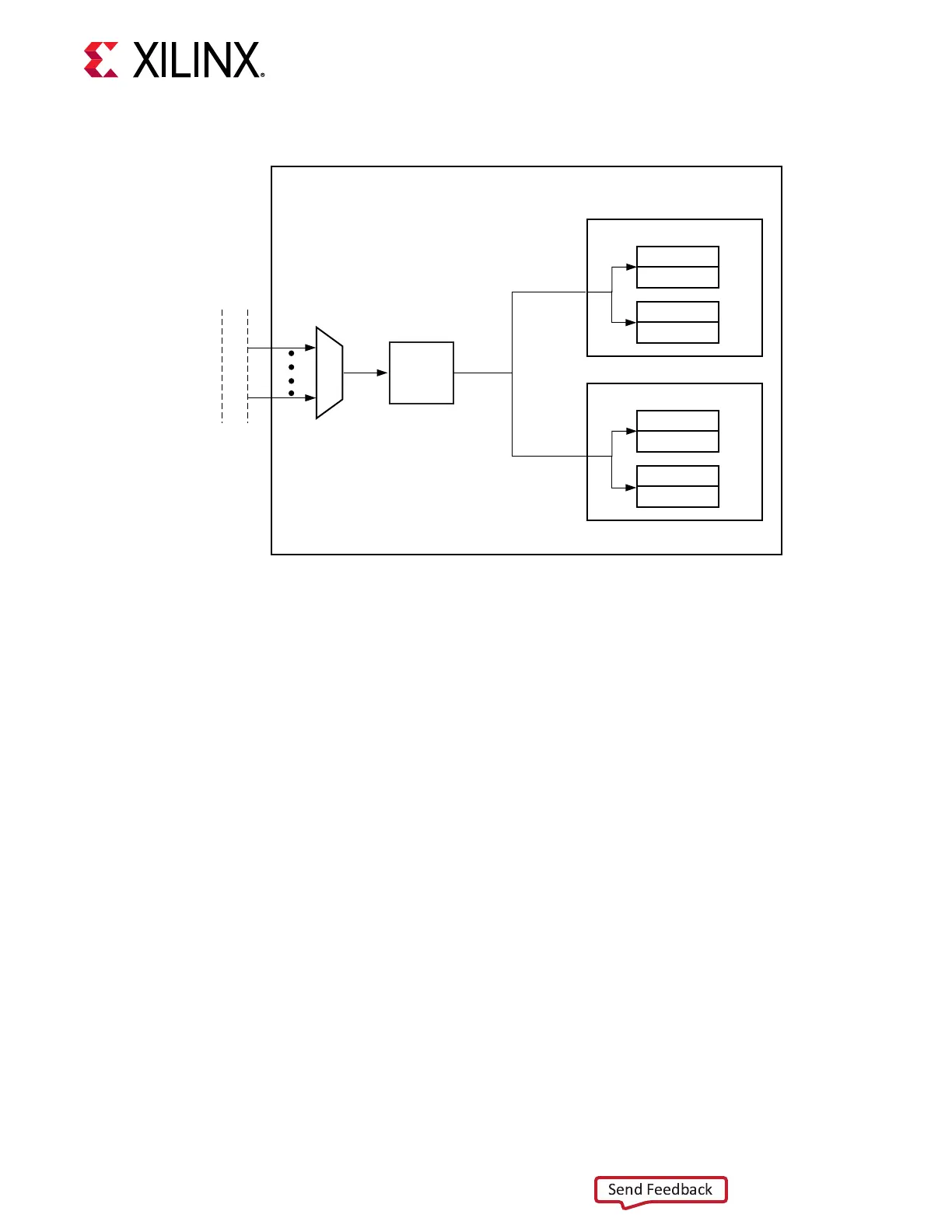
Figure 9: Internal Dual Clocking Architecture
LCPLL
GTM_DUAL
REFCLK Distribution
GTM Channel 0 (CH0)
TX PMA
TX PCS
RX PMA
RX PCS
GTM Channel 1 (CH1)
TX PMA
TX PCS
RX PMA
RX PCS
X20900-061418
The LCPLL input clock selecon is described in Reference Clock Selecon and Distribuon. The
LCPLL outputs feed the TX and RX clock divider blocks, which control the generaon of serial
and parallel clocks used by the PMA and PCS blocks. The LCPLL is shared between the TX and
RX datapaths.
The gure below illustrates a conceptual view of the LCPLL architecture. The input clock can be
divided by a factor of M before it is fed into the phase frequency detector. The feedback divider
N determines the voltage-controlled oscillator (VCO) mulplicaon rao. For line rates below
28.1 Gb/s (NRZ) and 56.2 Gb/s (PAM4), a fraconal-N divider is supported where the eecve
rao is a combinaon of the N factor plus a fraconal part. The LCPLL output frequency depends
on the sengs of LCPLLCLKOUT_RATE. When LCPLLCLKOUT_RATE is set to HALF, the output
frequency is half of the VCO frequency. When it is set to FULL, the output frequency is the same
as the VCO frequency. A lock indicator block compares the frequencies of the reference clock
and VCO feedback clock to determine if a frequency lock has been achieved.
Chapter 2: Shared Features
UG581 (v1.0) January 4, 2019 www.xilinx.com
Virtex UltraScale+ GTM Transceivers 19
 Loading...

