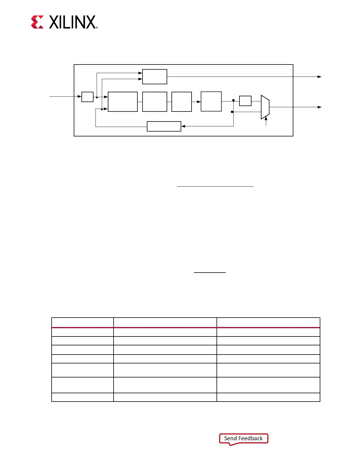
Figure 10: Internal Dual Clocking Architecture
/M
Phase
Frequency
Detector
Charge
Pump
/N-Fractional
Loop
Filter
Lock
Indicator
/2
VCO
PLL
CLKIN
PLL
LOCKED
PLL
CLKOUT
LCPLLCLKOUT_RATE
X20901-052418
The LCPLL VCO operates within 9.8 GHz—14.5 GHz. The Xilinx soware tool chooses the
appropriate LCPLL seng based on applicaon requirements. Equaon 2-1 shows how to
determine the PLL output frequency (GHz).
f
PLLClkout
= f
PLLClkin
*
N + FractionalDivider
M*LCPLLCLKOUT _ RATE
Equaon 2-2 shows how to determine the line rate (Gb/s).
f
LineRate
= f
PLLClkout
*Modulation
Equaon 2-3 and Equaon 2-4 show how to determine the fraconal divider presented in
Equaon 2-1.
FractionalDivider = N
SDM
+ 0. < FractionalPart >
FractionalPart
=
SDMDAT A
2
SDMWIDTH
The table below lists the allowable values.
Table 8: LCPLL Divider Settings
Factor Attribute or Port Valid Settings
M LCPLL_REFCLK_DIV 1, 2, 3, 4
N PLLFBDIV[7:0] 16–160 (Integer only)
LCPLLCLKOUT_RATE LCPLLCLKOUT_RATE 1'b1: 1 (Full), 1'b0: 2 (Half)
Modulation See TX Configurable Driver 2 (NRZ), 4 (PAM4)
N
SDM
SDMDATA[SDMWIDTH + 1:SDMWIDTH] Integer part of fractional divider. (Two’s
complement) –2, –1, 0, 1
SDMDATA SDMDATA[SDMWIDTH – 1:0] Fractional part of fractional divider.
0 – (2
24
– 1)
SDMWIDTH SDM_WIDTHSEL 16, 20, 24
Chapter 2: Shared Features
UG581 (v1.0) January 4, 2019 www.xilinx.com
Virtex UltraScale+ GTM Transceivers 20
 Loading...

