Ports and Attributes
The following tables dene the LCPLL ports and aributes, respecvely.
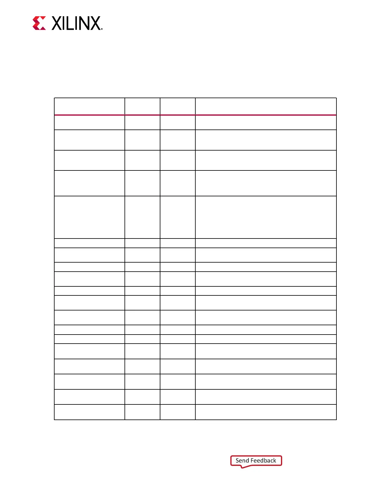
Table 9: LCPLL Ports
Port Direction
Clock
Domain
Description
GTGREFCLK2PLL In Clock Reference clock generated by the internal interconnect
logic. This input is reserved for internal testing purposes.
PLLFBCLKLOST Out PLLMONCLK A High on this signal indicates the feedback clock from the
LCPLL feedback divider to the phase frequency detector of
the LCPLL is lost
PLLFBDIV[7:0] In Async PLL feedback divider selection. Actual feedback divider value
is PLLFBDIV + 2. Valid values are from 14–158. (Actual divider
values are 160–160.)
PLLLOCK Out Async This active-High LCPLL frequency lock signal indicates that
the LCPLL frequency is within a predetermined tolerance.
The transceiver and its clock outputs are not reliable until
this condition is met.
PLLMONCLK In Clock Stable reference clock for the detection of the feedback and
reference clock signals to the LCPLL. The input reference
clock to the LCPLL or any output clock generated from the
LCPLL must not be used to drive this clock. This clock is
required only when using the PLLFBCLKLOST and
PLLREFCLKLOST ports. It does not affect the LCPLL lock
detection, reset, and power-down functions.
PLLPD
In Async An active-High signal powers down the LCPLL.
PLLREFCLKLOST Out PLLMONCLK A High on this signal indicates the reference clock to the
phase frequency detector of the LCPLL is lost.
PLLREFCLKMONITOR Out Clock PLL reference clock selection multiplexer output.
PLLRESET In Async This port is driven High and then deasserted to start the
LCPLL reset.
PLLRESETBYPASSMODE In Async Reserved. Tied Low.
PLLRESETDONE Out cfg_mclk Status signal that indicates when the PLL reset sequence is
complete.
PLLRESETMASK[1:0] In Async Bit 0 enables bit mask for PLL reset. Bit 1 enables bit mask
for PLL SDM reset.
PLLRSVDIN[15:0] In Reserved Reserved. This port must be set to 0x0000.
PLLRSVDOUT Out Async Reserved.
BGBYPASSB In Async Reserved. This port must be set to 1’b1. Do not modify this
value.
BGMONITORENB In Async Reserved. This port must be set to 1’b1. Do not modify this
value.
BGPDB In Async Reserved. This port must be set to 1’b1. Do not modify this
value.
BGRCALOVRD[4:0] In Async Reserved. This port must be set to 5’b11111. Do not modify
this value.
BGRCALOVRDENB In Async Reserved. This port must be set to 1’b1. Do not modify this
value.
Chapter 2: Shared Features
UG581 (v1.0) January 4, 2019 www.xilinx.com
Virtex UltraScale+ GTM Transceivers 21
 Loading...

