Table 46: TX Configurable Driver Ports (cont'd)
Port Dir
Clock
Domain
Description
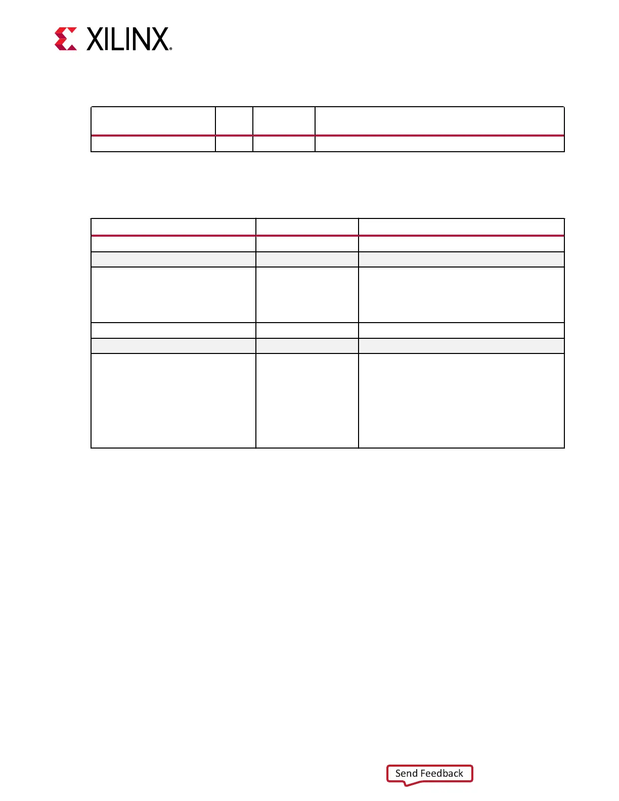
CH[0/1]_TXMUXDCDORWREN Input Async Reserved. Use the recommended value from the Wizard.
The following table denes the TX congurable driver aributes.
Table 47: TX Configurable Driver Attributes
Attribute Type Description
CH[0/1]_TX_ANA_CFG1 16-bit Reserved.
Bit Name Address Description
TXMODSEL [7] Driver output modulation control:
1’b0: PAM4 modulation.
1’b1: NRZ modulation.
CH[0/1]_TX_DRV_CFG0 16-bit Reserved.
Bit Name Address Description
TXEMPMAIN_INDEP [0] Allows independent control of the main cursor:
1’b0: The CH[0/1]_TXEMPMAIN coefficient is
automatically determined.
1’b1: CH[0/1]_TXEMPMAIN coefficient can be
independently set by the CH[0/1]_TXEMPMAIN
pins within the range specified in the pin
description.
Use Modes
The GTM TX has the ability to transmit serial data using two dierent modulaon schemes: NRZ
and PAM4. NRZ signals contains one bit of informaon per symbol, while PAM4 signals contain
two bits of informaon per symbol. Using PAM4 modulaon doubles the transmied data
bandwidth while maintaining the same unit interval (UI). To program the GTM TX to a desired
signal modulaon mode, the user must congure the aribute TXMODSEL for CH0 or CH1.
Chapter 3: Transmitter
UG581 (v1.0) January 4, 2019 www.xilinx.com
Virtex UltraScale+ GTM Transceivers 83
 Loading...

