MC81F4204
April 24, 2012 Ver.1.41 115
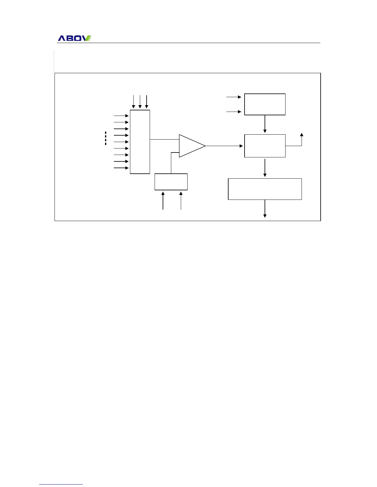
20. 12-BIT ADC
Clock
Selector
ADDRH (R), ADDRL (R)
-
+
EOC Flag
Control
Logic
Comparator
ADCH
(Select one input pin
of the assigned pins)
ADCLK
Input Pins
M
U
X
Reference
Voltage
Vref AVss
AN1
AN2
AN7
AN8
AN0
AN14
BGR
The 12-bit A/D converter (ADC) module uses successive approximation logic to convert analog levels
entering at one of the 1` input channels to equivalent 12-bit digital values. The analog input level must
lie between the V
REF
and V
SS
values. The A/D converter has the analog comparator with successive
approximation logic, D/A converter logic (resistor string type), A/D mode register (ADMR), 11
multiplexed analog data input pins (AD0-AD8,AD14,BGR), and 12-bit A/D conversion data output
register (ADDRH/ADDRL).
Figure 20-1 A/D Converter Block Diagram