MC81F4204
April 24, 2012 Ver.1.41 89
Xout and Xin pins can be used as normal pins
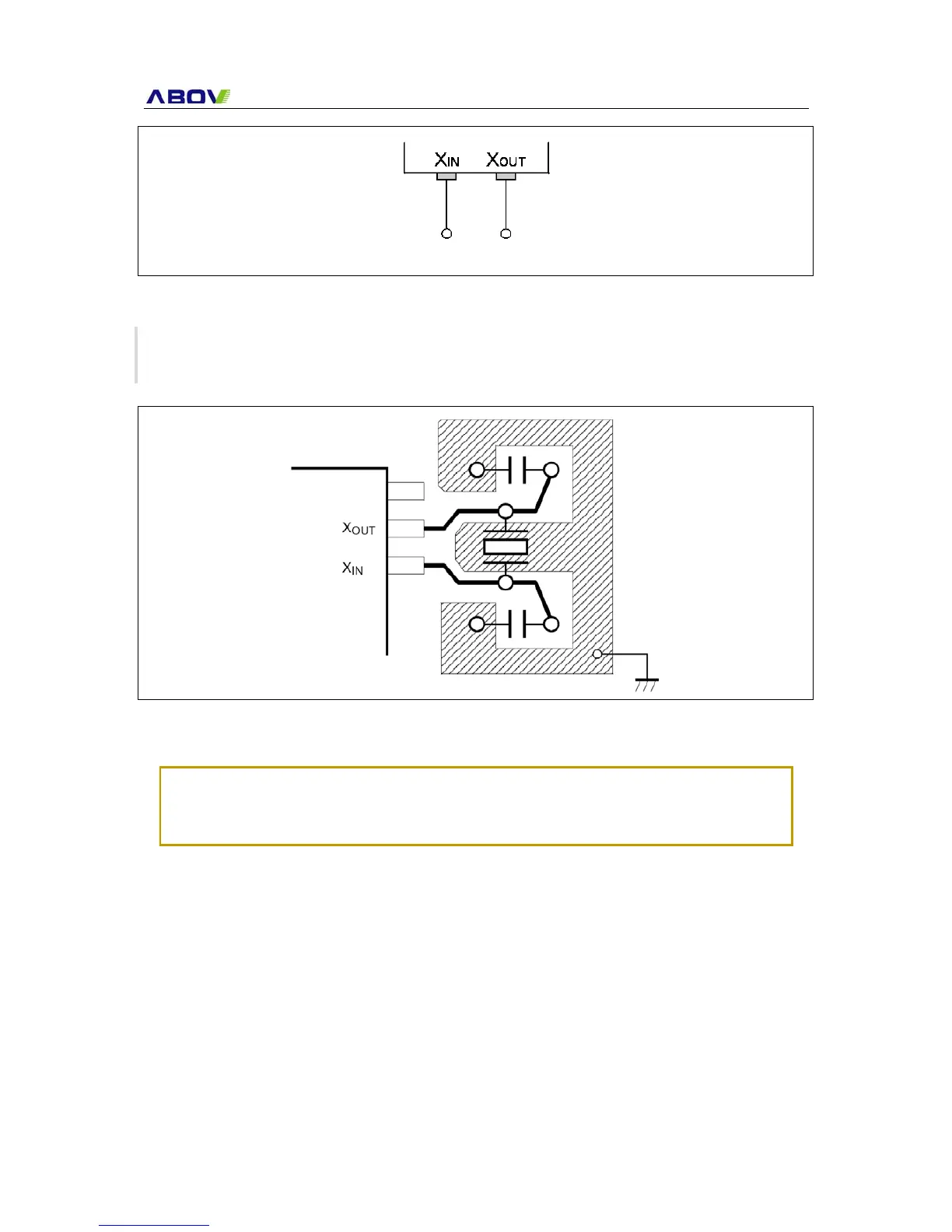
13.2 PCB Layout
For reference, here is a example layout for oscillator circuit.
Note :
Minimize the wiring length. Do not allow the wiring to intersect with other signal conductors.
Do not allow the wiring to come near changing high current. Set the potential of the
grounding position of the oscillator capacitor to that of VSS. Do not ground it to any ground
pattern where high current is present. Do not fetch signals from the oscillator.
Figure 13-4 Internal RC Oscillator
Figure 13-5 Layout of Oscillator PCB circuit