Theory of Operation 8
16900A, 16902A, and 16903A Service Guide 107
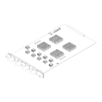
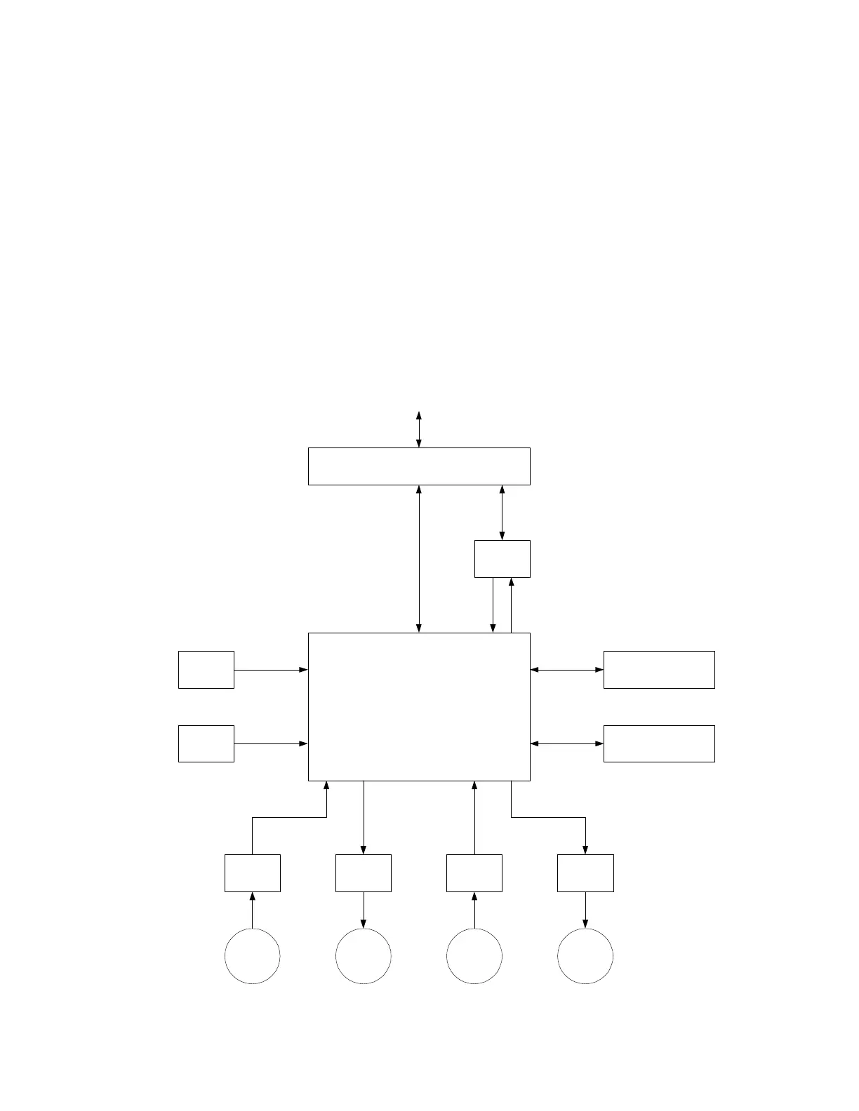
I/O board
The following I/O (input/output) board subsystem block
diagram includes:
• FPGA (more on page 112)
• Multiframe input/output (more on page 113)
• Target control port (more on page 113)
• Trigger IN/OUT (more on page 113)
• Clock IN (more on page 114)
• Calibration OUT (more on page 114)
FPGA
120 pin CONNECTOR
to MIB (module interface board)
100MHZ
SOURCE
MULTIFRAME
INPUT/OUTPUT
CONNECTORS
TARGET CONTROL
PORT CONNECTOR
EPROM
FLAGS
BUFFER
PORT IN
BNC
CLOCK IN
BNC
PORT OUT
BNC
CAL OUT
BNC
10X
BUFFER
DAC &
BUFFER
50 ohm
BUFFER
50 ohm
BUFFER
CONTENT:
1.6 GHz Correlator
Arm/trig/flag router
100 MHz clocking
IO interface
TO MODULE CONNECTORS
 Loading...