12 Agilent N5181A/82A MXG Signal Generators User’s Guide
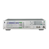
Signal Generator Overview
Rear Panel Overview
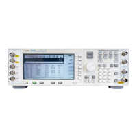
Digital Modulation Connectors (vector models only)
I OUT, QOUT, OUT, OUT
EXT CLOCK
EVENT 1
Connector Type: female BNC Impedance: 50Ω
DC- coupled
Signal
I OUT The analog, in- phase component of I/Q modulation from the internal baseband generator.
Q OUT The analog, quadrature- phase component of I/Q modulation from the internal baseband
generator.
OUT
Used in conjunction with the I OUT connector to provide a balanced
a
baseband stimulus.
a
Balanced signals are signals present in two separate conductors that are symmetrical relative to ground, and are opposite in polarity
(180 degrees out of phase).
OUT
Used in conjunction with the Q OUT connector to provide a balanced
a
baseband stimulus.
Damage Levels > 1 Vrms DC Origin Offset typically <10 mV
Output Signal Levels into a 50Ω Load
• 0.5V
pk
, typical, corresponds to one unit length of the I/Q vector
• 0.69V
pk
(2.84 dB), typical, maximum crest factor for peaks for π/4 DQPSK, alpha = 0.5
• 0.71V
pk
(3.08 dB), typical, maximum crest factor for peaks for π/4 DQPSK, alpha = 0.35
• Typically 1V
p- p
maximum
Connector female BNC Impedance nominally 50Ω
Signal An externally supplied TTL or CMOS bit clock signal where the rising edge aligns with the
beginning data bit.
The falling edge is used to clock external signals.
This signal is used with digital modulation applications.
Damage Levels > +8 and < −4V Maximum Clock Rate 50 MHz
Connector female BNC Impedance: nominally 50Ω
Signal A pulse that can be used to trigger the start of a data pattern, frame, or timeslot.
Adjustable to ± one timeslot; resolution = one bit
Markers
Each Arb- based waveform point has a marker on/off condition associated with it.
Marker 1 level = +3.3V CMOS high (positive polarity selected); –3.3V CMOS low (negative
polarity selected).
Output on this connector occurs whenever Marker 1 is on in an Arb- based waveform (see
“Using Waveform Markers” on page 82).
Damage Levels >+8 and <−4V
 Loading...