System Control
ARM DDI 0363G Copyright © 2006-2011 ARM Limited. All rights reserved. 4-44
ID073015 Non-Confidential
• ARM recommends that any instruction that changes bits [20:16] is
followed by an
ISB
instruction to ensure that the changes have taken
effect before any dependent instructions are executed.
Configurations Available in all processor configurations.
Attributes See Table 4-25.
This register is implemented from the r1pn releases of the processor. Attempting to access this
register in r0pn releases of the processor results in an Undefined Instruction exception.
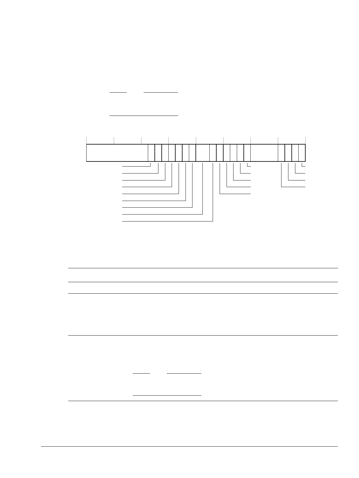
Figure 4-28 shows the Secondary Auxiliary Control Register bit assignments.
Figure 4-28 Secondary Auxiliary Control Register bit assignments
Table 4-25 shows the Secondary Auxiliary Control Register bit assignments.
ReservedReserved
31
22
21
19 18
17
16 15 14 13 12 11 7 3 2 1 01020 9 48
DR2B
DF6DI
DF2DI
DOODPFP
DDI
ATCMRMW
ATCMECC
IDC
DZC
IOC
UFC
OFC
IXC
DOOFMACS
BTCMRMW
B0TCMECC
Reserved
DCHE
23
Table 4-25 Secondary Auxiliary Control Register bit assignments
Bits Name Function
[31:23] - SBZ.
[22] DCHE
Disable hard-error support in the caches:
a
0
= Enabled. The cache logic recovers from some hard errors. You must not use this value on
revisions r1p2 or earlier of the processor.
1
= Disabled. Most hard errors in the caches are fatal. This is the reset value.
See Hard errors on page 8-5 for more information.
[21]
DR2B
b
Enable random 2-bit error generation in cache RAMs. This bit has no effect unless ECC is
configured, see Configurable options on page 1-6:
0
= Disabled. This is the reset value.
1
= Enabled.
This bit controls error generation logic during system validation. A synthesized ASIC
typically does not have such models and this bit is therefore redundant for ASICs.
[20] DF6DI
F6 dual issue control:
c
0
= Enabled. This is the reset value.
1
= Disabled.