Debug
ARM DDI 0363G Copyright © 2006-2011 ARM Limited. All rights reserved. 12-21
ID073015 Non-Confidential
Table 12-13 shows the DBGVCR bit assignments.
12.4.9 Debug State Cache Control Register
The DBGDSCCR Register characteristics are:
Purpose Controls the L1 cache behavior when the processor is in debug state.
Usage constraints For information on the usage model of the DBGDSCCR register, see
Cache debug on page 12-53.
Configurations Available in all processor configurations.
Attributes See Table 12-14 on page 12-22.
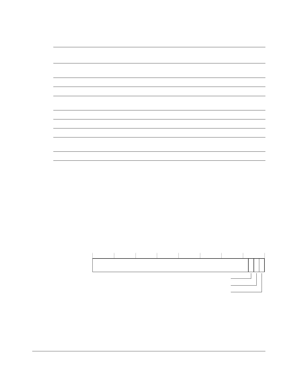
Figure 12-8 shows the DBGDSCCR bit assignments.
Figure 12-8 DBGDSCCR Register bit assignments
For information on the usage model of the DBGDSCCR register, see Cache debug on
page 12-53.
Table 12-13 DBGVCR Register bit assignments
Bits Name
Reset
value
Normal
address
High vectors
address
Function Access
[31:8] - 0 -
-
Do not modify on writes. On reads,
the value returns zero.
RAZ or
SBZP
[7] FIQ 0
0x0000001C 0xFFFF001C
Vector catch enable. RW
[6] IRQ -
0x00000018
a
0xFFFF0018
a
Vector catch enable. -
[5] - 0 -
-
Do not modify on writes. On reads,
the value returns zero.
RAZ or
SBZP
[4] Data Abort 0
0x00000010 0xFFFF0010
Vector catch enable. RW
[3] Prefetch Abort 0
0x0000000C 0xFFFF000C
Vector catch enable. RW
[2] SVC 0
0x00000008 0xFFFF0008
Vector catch enable. RW
[1] - 0
0x00000004 0xFFFF0004
Vector catch enable, Undefined
instruction.
RW
[0] Reset 0
0x00000000 0xFFFF0000
Vector catch enable. RW
a. If the VIC interface is enabled, the address is the last IRQ handler address supplied by the VIC, whether or not high vectors
are in use.
31
2131 0
Not write-through
Reserved
3
Instruction cache line-fill
Data cache line-fill