IPC@CHIP SC123/SC143
Hardware Manual V1.06 [18.02.2010]
©2000-2008 BECK IPC GmbH Page 54
11 Application Examples
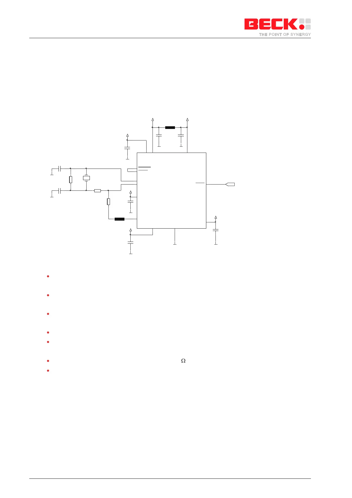
11.1 Minimum Circuit Requirements
Figure 11-1 shows the minimum hardware requirements for the SC1x3 to boot up and run properly.
Place all these parts as close as possible to the SC1x3. Pay attention to chapter 5.
3.3V
C2
C6
GND
3.3V
GND
GND
C8
C1
A3.3V
GND
Supervisory Circuit
GND
Y1
25MHz
R2
470
R3
120
C5
22pF
3.3V
L2
3000@80MHz
R1
1M
C7
IC1
SC1x3
U6
U5
J1
H1
H2
R8
VDDA
VDD
UCSOUT
UCSIN
RSTIN
VSS
XIN
XOUT
CPUCLK
VDD
VDD
VDD
VDD
GND
L1
GND
C3
3.3V
AGND
GND
C4
22pF
3.3V
Figure 11-1: Minimum Circuit Requirements for SC1x3
The Trace between UCSIN# and UCSOUT# is very important for the boot process, see chapter 4.3 and
11.3.
A Supervisory Circuit is recommended to ensure that the reset is asserted until the power supply is stable in
the recommended range.
The feedback line between CPUCLK and XOUT with the resistor R2 and the inductivity L2 is important for
the SC1x3 to reliably start the oscillation of the internal clock frequency.
Place all parts as short as possible to the SC1x3.
Don’t load CPUCLK with any capacity or circuit input. Short raise and fall times of the CPUCLK signal are
important for correct working of the internal SDRAM. See chapter 12.
The value of R3 depends on EMC requirements, 120 is a suggestion.
A crystal with 25MHz ±100ppm is recommended