IPC@CHIP SC123/SC143
Hardware Manual V1.06 [18.02.2010]
©2000-2008 BECK IPC GmbH Page 50
9 Routing and Placement Rules
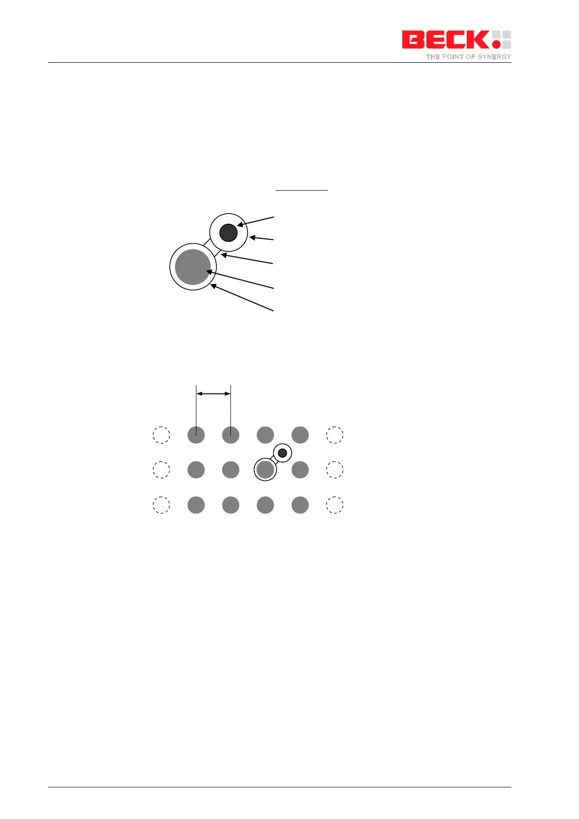
9.1 PCB Board Design suggestion for SC123/SC143
Via Features
0.25mm finished plated through hole
(covered with soldering mask)
0.6 mm Annular Pad
0.175+ mm line between pads
0.71 mm soldering opening
Copper pad 0.71 mm
Figure 9-1: PCB Board Design suggestion
Figure 9-2: PCB Board Design suggestion