Table 87 (Continuation): Modbus memory map: Programming alarms 1 and 2.
Programming alarms 1 and 2
Configuration variable
Address
Valid data margin
Default
value
Relay 1 Relay 2
latch 2AFF 2B09
0 : No
1: Yes
0
Disconnection delay 2B00 2B0A 0 - 9999 seconds 0
Contacts status 2B01 2B0B
0 : Normally open
1: Normally closed
0
7.3.8.14.- Programming alarms 3 and 4 (Digital outputs T1 and T2)
Table 88: Modbus memory map: Programming alarms 3 and 4.
Programming alarms 3 and 4
Configuration variable
Address
Valid data margin
Default
value
Relay 1 Relay 2
Kilowatts per impulse 2B0C-2B0D 2B16-2B17 Table 52 0
Variable code 2B10 2B1A Table 43, Table 44 and Table 51 0
Pulse width 2B11 2B1B 30 - 400 ms 100 ms
7.3.8.15.- Digital inputs
Table 89: Modbus memory map: Configuration of digital inputs.
Configuration variable
Address
Valid data margin
Default
value
Input 1 Input 2
Operating mode
(10)
2B66 2B67
0: Tariff
1: Logic state
2: Maximum demand synchronism pulse
(11)
0
(10)
If Input 1 is configured as a tariff and Input 2 is configured as a logic state (or vice versa) we will only have 2
tariffs.
(11)
Option available on digital input 1.
We can also read the status of the digital inputs when they are in logic mode:
The Function 0x04 is implemented for this variable.
Table 90: Modbus memory map: Status of the digital inputs (Logic state mode)
Status of digital inputs
Variable Address Default value
Status of digital inputs 4E20 -
The variable format is shown in Table 91:
Table 91: Variable format: Status of digital inputs.
Bit 7 Bit 6 Bit 5 Bit 4 Bit 3 Bit 2 Bit 1 Bit 0
0 0 0 0 0 0
Input 2
0: OFF
1: ON
Input 1
0: OFF
1: ON
84
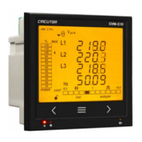
CVM-C11
Instruction Manual
 Loading...