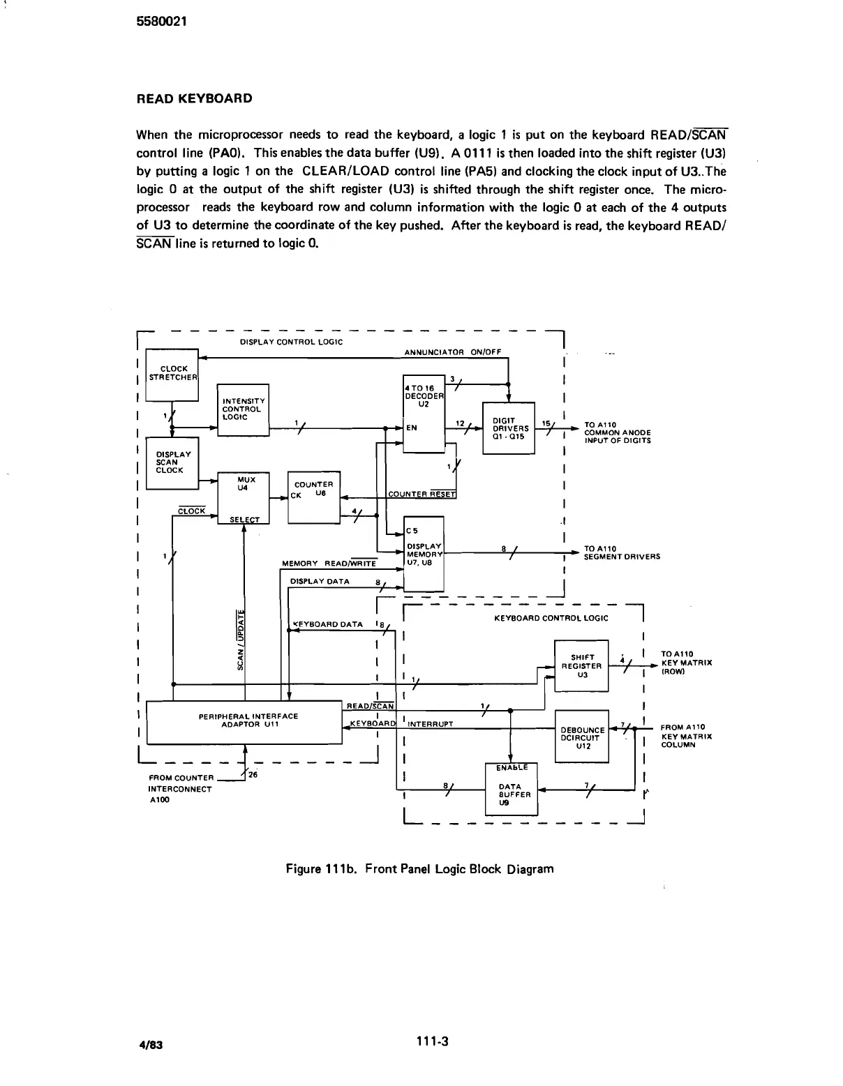
READKEYBOARD
When the microprocessor needs to read the keyboard,
a
logic 1
is
put on the keyboard READISCAN
control line (PAO). This enables the data buffer (U9). A 01 11
is
then loaded into the shift register (U3)
by putting
a
logic 1 on the CLEARILOAD control line (PA5) and clocking the clock input of U3..The
logic 0
at
the output of the shift register (U3)
is
shifted through the shift register once. The micro-
processor reads the keyboard row and column information with the logic
0
at
each of the
4
outputs
of U3 to determine the coordinate of the key pushed. After the keyboard
is
read, the keyboard READ1
SCAN line
is
returned to logic
0.
Figure 11 1 b. Front Panel Logic Block Diagram
Scans by ArtekMedia © 2007