TESTS
01
200
MHz
Self Test
This
test
sets
the VCO to 400 MHz, divides
it
by two, and counts the 200 MHz
output from the divider.
It
checks the count chain, VCO and VCO phase lock circuitry, and the gate
generator.
02
8's
Test This will light all LED's, annunicators, and decimal points. It checks that everything on the
display
is
lit, the intensity of the display, and the alignment of the LED's and annunciators.
03
Display Segment Test
This lights one segment of each digit, and one annunciator
at
a
time, cycling
through all segments. The cycle rate can be adjusted with the sample rate pot. It verifies that each
segment of the display, segment drivers and display multiplexer, operate properly and independ-
ently.
04
Display Digit Test This lights one entire digit, and
its
decimal point,
at
a
time. It cycles through
all digits and annunciators. The cycle rate
is
determined by the sample rate pot. It checks each digit
and digit driver independently, and verifies operation of the display multiplexer.
05
Keyboard Test This will display the coordinates of each key
as
it
is
pressed.
It
also generates
a
unique signature for each key, so the keyboard can be checked without the display. Test 05 may
be entered by keyboard or by momentarily tying A108
TP1 to A105 TP8 (or to A108, U5, pin 25).
This makes
it
possible to enter the keyboard
test
for troubleshooting even if the keyboard is not
operating well enough to enter the test in
a
normal manner. Test 05 checks the keyboard, keyboard
interrupt, and keyboard decode circuitry. The coordinates and signatures for each key are shown in
figure 6-5.
06
Converter Ramp Test
Test 06 continuously ramps the Band 3 Converter DAC from
0 to 27 GHz,
in 2 MHz (LSB) steps. It also generates
a
signature for each of the inputs to the DAC. (See figure
6-6).
It
can be used to test the yig DAC, yig drivers, yig, and Band 3 RF level circuits.
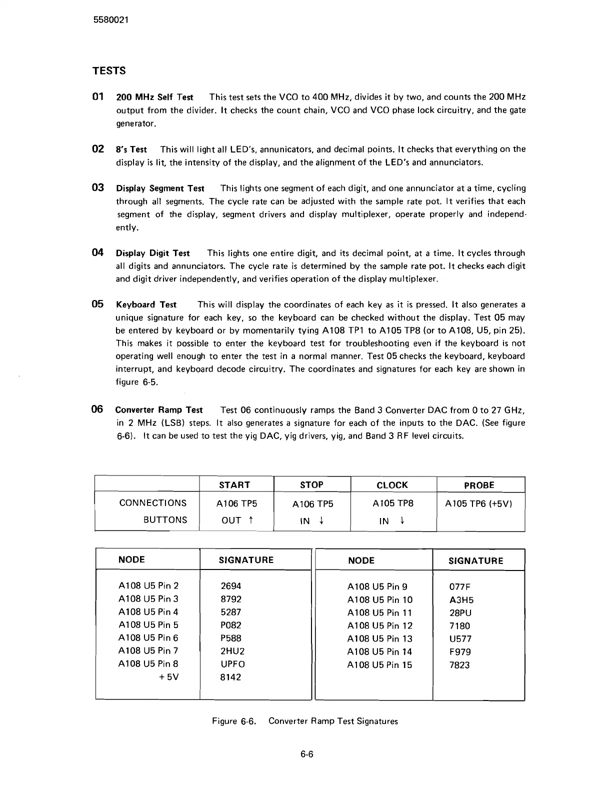
I
BUTTONS
1
OUT
?
1
IN
-1
1
IN
-1
I
I
CONNECTIONS
Figure 6-6.
Converter Ramp Test Signatures
6-6
START
A1 06 TP5
NODE
A1 08 U5 Pin 2
A108 U5 Pin 3
A108 U5 Pin 4
A1 08 U5 Pin 5
A108 U5 Pin 6
A108 U5 Pin 7
A108 U5 Pin 8
+
5V
STOP
A106 TP5
SIGNATURE
2694
8792
5287
PO82
P588
2HU2
UPFO
8142
NODE
A108 U5 Pin 9
A108 U5 Pin 10
A108 U5 Pin 11
A108 U5 Pin 12
A108 U5 Pin 13
A108 U5 Pin 14
A108 U5 Pin 15
SIGNATURE
077F
A3H5
28PU
7180
U577
F979
7823
CLOCK
A 105 TP8
PROBE
A105 TP6
(+5V)
Scans by ArtekMedia © 2007